MCP651EV-VOS Microchip Technology, MCP651EV-VOS Datasheet - Page 4
MCP651EV-VOS
Manufacturer Part Number
MCP651EV-VOS
Description
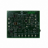
BOARD EVAL OP AMP MCP651
Manufacturer
Microchip Technology
Series
mCal Technologyr
Specifications of MCP651EV-VOS
Channels Per Ic
1 - Single
Amplifier Type
General Purpose
Output Type
Single-Ended, Rail-to-Rail
Slew Rate
30 V/µs
Current - Output / Channel
100mA
Operating Temperature
-40°C ~ 125°C
Current - Supply (main Ic)
6mA
Voltage - Supply, Single/dual (±)
2.5 V ~ 5.5 V
Board Type
Fully Populated
Utilized Ic / Part
MCP651
Processor To Be Evaluated
MCP651
Maximum Operating Temperature
+ 125 C
Minimum Operating Temperature
- 40 C
Operating Supply Voltage
2.5 V to 5.5 V
Tool Type
Evaluation Board
Core Architecture
PIC
Cpu Core
PIC
Data Bus Width
8 bit
Lead Free Status / RoHS Status
Lead free / RoHS Compliant
-3db Bandwidth
-
Lead Free Status / Rohs Status
Lead free / RoHS Compliant
Available stocks
Company
Part Number
Manufacturer
Quantity
Price
Company:

Part Number:
MCP651EV-VOS
Manufacturer:
Microchip Technology
Quantity:
135
Company:
Part Number:
MCP651EV-VOS
Manufacturer:
MICROCHIP
Quantity:
12 000


MCP6V01/2/3
TABLE 1-1:
TABLE 1-2:
DS22058C-page 4
Electrical Characteristics: Unless otherwise indicated, T
V
Output
Maximum Output Voltage Swing
Output Short Circuit Current
Power Supply
Supply Voltage
Quiescent Current per amplifier
POR Trip Voltage
Note 1:
Electrical Characteristics: Unless otherwise indicated, T
V
Amplifier AC Response
Gain Bandwidth Product
Slew Rate
Phase Margin
Amplifier Noise Response
Input Noise Voltage
Input Noise Voltage Density
Input Noise Current Density
Amplifier Distortion (Note 1)
Intermodulation Distortion (AC)
Amplifier Step Response
Start Up Time
Offset Correction Settling Time
Output Overdrive Recovery Time
Note 1:
OUT
OUT
= V
= V
2:
2:
DD
DD
/2, V
/2, V
Set by design and characterization. Due to thermal junction and other effects in the production environment, these parts
can only be screened in production (except TC
Figure 2-18
These parameters were characterized using the circuit in
tone at DC and a residual tone at1 kHz; all other IMD and clock tones are spread by the randomization circuitry.
t
Parameters
ODR
Parameters
L
L
includes some uncertainty due to clock edge timing.
= V
= V
DC ELECTRICAL SPECIFICATIONS (CONTINUED)
AC ELECTRICAL SPECIFICATIONS
DD
DD
/2, R
shows how V
/2, R
L
L
= 20 kΩ to V
= 20 kΩ to V
CMR
GBWP
Sym
t
changed across temperature for the first three production lots.
IMD
IMD
t
t
PM
ODR
SR
STR
E
E
e
e
STL
L
L
i
ni
, and CS = GND (refer to
, C
ni
ni
ni
ni
V
OL
L
Sym
V
V
I
I
= 60 pF, and CS = GND (refer to
POR
SC
SC
I
, V
DD
Q
Min Typ Max Units
—
—
—
—
—
—
—
—
—
—
—
—
—
OH
0.79
120
500
300
100
A
A
1.3
0.5
2.5
0.6
V
65
45
<1
<1
1
SS
= +25°C, V
= +25°C, V
; see Appendix B: “Offset Related Test Screens”).
Min
1.15
200
1.8
—
—
+ 15
—
—
—
—
—
—
—
—
—
—
—
—
—
Figure
Figure 1-5
DD
DD
nV/√Hz f < 2.5 kHz
nV/√Hz f = 100 kHz
Typ
±22
300
fA/√Hz
µV
µV
±7
µV
µV
—
—
—
MHz
V/µs
µs
µs
µs
= +1.8V to +5.5V, V
= +1.8V to +5.5V, V
°
P-P
P-P
PK
PK
1-7.
V
G = +1
f = 0.01 Hz to 1 Hz
f = 0.1 Hz to 10 Hz
V
V
V
G = +1, V
V
G = -100, ±0.5V input overdrive to V
V
and
Figure 2-37
DD
Figure 1-5
CM
CM
OS
OS
IN
Max
1.65
400
5.5
—
—
50% point to V
− 15
Figure
within 50 µV of its final value
within 50 µV of its final value
tone = 50 mV
tone = 50 mV
IN
1-6).
Units
step of 2V,
and
and
SS
SS
mV
mA
mA
µA
V
V
= GND, V
= GND, V
Figure
© 2008 Microchip Technology Inc.
Figure 2-38
Conditions
PK
PK
OUT
G = +2, 0.5V input overdrive
V
V
I
at 1 kHz, G
at 1 kHz, G
O
DD
DD
90% point (Note 2)
= 0
1-6).
= 1.8V
= 5.5V
CM
CM
Conditions
= V
= V
show both an IMD
N
N
DD
DD
= 1, V
= 1, V
/3,
/3,
DD
/2,
DD
DD
= 1.8V
= 5.5V
Related parts for MCP651EV-VOS
Image
Part Number
Description
Manufacturer
Datasheet
Request
R

Part Number:
Description:
Manufacturer:
Microchip Technology Inc.
Datasheet:
Part Number:
Description:
Manufacturer:
Microchip Technology Inc.
Datasheet:
Part Number:
Description:
Manufacturer:
Microchip Technology Inc.
Datasheet:
Part Number:
Description:
Manufacturer:
Microchip Technology Inc.
Datasheet:
Part Number:
Description:
Manufacturer:
Microchip Technology Inc.
Datasheet:
Part Number:
Description:
Manufacturer:
Microchip Technology Inc.
Datasheet:
Part Number:
Description:
Manufacturer:
Microchip Technology Inc.
Datasheet:
Part Number:
Description:
Manufacturer:
Microchip Technology Inc.
Datasheet: