MCP651EV-VOS Microchip Technology, MCP651EV-VOS Datasheet - Page 22
MCP651EV-VOS
Manufacturer Part Number
MCP651EV-VOS
Description
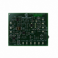
BOARD EVAL OP AMP MCP651
Manufacturer
Microchip Technology
Series
mCal Technologyr
Specifications of MCP651EV-VOS
Channels Per Ic
1 - Single
Amplifier Type
General Purpose
Output Type
Single-Ended, Rail-to-Rail
Slew Rate
30 V/µs
Current - Output / Channel
100mA
Operating Temperature
-40°C ~ 125°C
Current - Supply (main Ic)
6mA
Voltage - Supply, Single/dual (±)
2.5 V ~ 5.5 V
Board Type
Fully Populated
Utilized Ic / Part
MCP651
Processor To Be Evaluated
MCP651
Maximum Operating Temperature
+ 125 C
Minimum Operating Temperature
- 40 C
Operating Supply Voltage
2.5 V to 5.5 V
Tool Type
Evaluation Board
Core Architecture
PIC
Cpu Core
PIC
Data Bus Width
8 bit
Lead Free Status / RoHS Status
Lead free / RoHS Compliant
-3db Bandwidth
-
Lead Free Status / Rohs Status
Lead free / RoHS Compliant
Available stocks
Company
Part Number
Manufacturer
Quantity
Price
Company:

Part Number:
MCP651EV-VOS
Manufacturer:
Microchip Technology
Quantity:
135
Company:
Part Number:
MCP651EV-VOS
Manufacturer:
MICROCHIP
Quantity:
12 000


MCP6V01/2/3
4.1.2
Figure 4-2
during the Normal Mode of operation (φ
capacitor (C
Since the Null Amplifier has very high gain, it
dominates the signal seen by the Main Amplifier. This
greatly reduces the impact of the Main Amplifier’s input
FIGURE 4-2:
Figure 4-3
during the Auto-zeroing Mode of operation (φ
signal goes directly through the Main Amplifier, and the
flywheel capacitor (C
tion on the Main Amplifier’s offset.
The Null Amplifier uses its own high open loop gain to
drive the voltage across C
offset voltage is almost zero. Because the principal
input is connected to V
corrects the offset at the current common mode input
voltage (V
the DC CMRR and PSRR very high also.
FIGURE 4-3:
4.1.3
The MCP6V01/2/3 op amps will show intermodulation
distortion (IMD), products when an AC signal is
present.
The signal and clock can be decomposed into sine
wave tones (Fourier series components). These tones
interact with the auto-zeroing circuitry’s non-linear
DS22058C-page 22
V
V
V
V
IN
IN
IN
IN
CM
+
–
+
–
shows the connections between amplifiers
shows the connections between amplifiers
AUTO-ZEROING ACTION
INTERMODULATION DISTORTION
(IMD)
H
) and supply voltage (V
) corrects the Null Amplifier’s input offset.
C
C
H
H
FW
Normal Mode of Operation (
Auto-zeroing Mode of Operation (
) maintains a constant correc-
IN
H
+, the auto-zeroing action
to the point where its input
Amp.
Amp.
Null
Null
DD
). This makes
1
). The hold
2
C
C
). The
FW
FW
φ
1
); Equivalent Amplifier Diagram.
φ
2
); Equivalent Diagram.
Amp.
Amp.
Main
Main
offset voltage on overall performance. Essentially, the
Null Amplifier and Main Amplifier behave as a regular
op amp with very high gain (A
voltage (V
Since these corrections happen every 100 µs, or so,
we also minimize slow errors, including offset drift with
temperature (ΔV
aging.
response to produce IMD tones at sum and difference
frequencies. IMD distortion tones are generated about
all of the square wave clock’s harmonics.
Clock randomization spreads the IMD tones across the
frequency spectrum, but cannot eliminate them. The
spread energy is low and is not correlated with the sig-
nal of interest, so it is not of concern for most precision
applications. See
OS
).
V
V
NC
NC
REF
REF
OS
Figure 2-37
/ΔT
A
© 2008 Microchip Technology Inc.
), 1/f noise, and input offset
Output
Output
Buffer
Buffer
and
OL
) and very low offset
Figure
2-38.
V
V
OUT
OUT
Related parts for MCP651EV-VOS
Image
Part Number
Description
Manufacturer
Datasheet
Request
R

Part Number:
Description:
Manufacturer:
Microchip Technology Inc.
Datasheet:
Part Number:
Description:
Manufacturer:
Microchip Technology Inc.
Datasheet:
Part Number:
Description:
Manufacturer:
Microchip Technology Inc.
Datasheet:
Part Number:
Description:
Manufacturer:
Microchip Technology Inc.
Datasheet:
Part Number:
Description:
Manufacturer:
Microchip Technology Inc.
Datasheet:
Part Number:
Description:
Manufacturer:
Microchip Technology Inc.
Datasheet:
Part Number:
Description:
Manufacturer:
Microchip Technology Inc.
Datasheet:
Part Number:
Description:
Manufacturer:
Microchip Technology Inc.
Datasheet: