MCP651EV-VOS Microchip Technology, MCP651EV-VOS Datasheet - Page 26
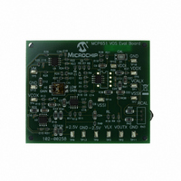
MCP651EV-VOS
Manufacturer Part Number
MCP651EV-VOS
Description
BOARD EVAL OP AMP MCP651
Manufacturer
Microchip Technology
Series
mCal Technologyr
Specifications of MCP651EV-VOS
Channels Per Ic
1 - Single
Amplifier Type
General Purpose
Output Type
Single-Ended, Rail-to-Rail
Slew Rate
30 V/µs
Current - Output / Channel
100mA
Operating Temperature
-40°C ~ 125°C
Current - Supply (main Ic)
6mA
Voltage - Supply, Single/dual (±)
2.5 V ~ 5.5 V
Board Type
Fully Populated
Utilized Ic / Part
MCP651
Processor To Be Evaluated
MCP651
Maximum Operating Temperature
+ 125 C
Minimum Operating Temperature
- 40 C
Operating Supply Voltage
2.5 V to 5.5 V
Tool Type
Evaluation Board
Core Architecture
PIC
Cpu Core
PIC
Data Bus Width
8 bit
Lead Free Status / RoHS Status
Lead free / RoHS Compliant
-3db Bandwidth
-
Lead Free Status / Rohs Status
Lead free / RoHS Compliant
Available stocks
Company
Part Number
Manufacturer
Quantity
Price
Company:

Part Number:
MCP651EV-VOS
Manufacturer:
Microchip Technology
Quantity:
135
Company:
Part Number:
MCP651EV-VOS
Manufacturer:
MICROCHIP
Quantity:
12 000


MCP6V01/2/3
4.3.9
In order to achieve DC precision on the order of ±1 µV,
many physical errors need to be minimized. The design
of the Printed Circuit Board (PCB), the wiring, and the
thermal environment has a strong impact on the
precision achieved. A poor PCB design can easily be
more than 100 times worse than the MCP6V01/2/3 op
amps minimum and maximum specifications.
4.3.9.1
Any time two dissimilar metals are joined together, a
temperature dependent voltage appears across the
junction (the Seebeck or thermo-junction effect). This
effect is used in thermocouples to measure tempera-
ture. The following are examples of thermo-junctions
on a PCB:
• Components (resistors, op amps, …) soldered to
• Wires mechanically attached to the PCB
• Jumpers
• Solder joints
• PCB vias
Typical thermo-junctions have temperature to voltage
conversion coefficients of 10 to 100 µV/°C (sometimes
higher).
There are three basic approaches to minimizing
thermo-junction effects:
• Minimize thermal gradients
• Cancel thermo-junction voltages
• Minimize difference in thermal potential between
DS22058C-page 26
a copper pad
metals
PCB DESIGN FOR DC PRECISION
Thermo-junctions
4.3.9.2
Figure 4-11
and inverting gain amplifier circuits on one schematic.
Usually, to minimize the input bias current related off-
set, R
The guard traces (with ground vias at the ends) help
minimize the thermal gradients. The resistor layout
cancels the resistor thermal voltages, assuming the
temperature gradient is constant near the resistors:
EQUATION 4-2:
FIGURE 4-11:
for Single Non-inverting and Inverting Amplifiers.
Where:
Note:
V
V
G
G
1
M
P
M
P
is chosen to be R
V
V
=
=
M
P
Changing the orientation of the resistors
will usually cause a significant decrease in
the cancellation of the thermal voltages.
shows the recommended non-inverting
V
MCP6V01
Non-inverting and Inverting Amplifier
Layout for Thermo-junctions
OUT
R
1 + G
magnitude
V
R3
R2
R1
OS
3
/R
R
R
≈ -V
≈ V
1
2
is neglected
2
M
U
, inverting gain magnitude
P
, non-inverting gain
PCB Layout and Schematic
1
M
G
© 2008 Microchip Technology Inc.
G
2
P
||R
,
M
, V
R
3
.
3
V
U1
M
P
= GND
= GND
V
OUT
V
OUT
Related parts for MCP651EV-VOS
Image
Part Number
Description
Manufacturer
Datasheet
Request
R

Part Number:
Description:
Manufacturer:
Microchip Technology Inc.
Datasheet:
Part Number:
Description:
Manufacturer:
Microchip Technology Inc.
Datasheet:
Part Number:
Description:
Manufacturer:
Microchip Technology Inc.
Datasheet:
Part Number:
Description:
Manufacturer:
Microchip Technology Inc.
Datasheet:
Part Number:
Description:
Manufacturer:
Microchip Technology Inc.
Datasheet:
Part Number:
Description:
Manufacturer:
Microchip Technology Inc.
Datasheet:
Part Number:
Description:
Manufacturer:
Microchip Technology Inc.
Datasheet:
Part Number:
Description:
Manufacturer:
Microchip Technology Inc.
Datasheet: