MCP6V01DM-VOS Microchip Technology, MCP6V01DM-VOS Datasheet - Page 10
MCP6V01DM-VOS
Manufacturer Part Number
MCP6V01DM-VOS
Description
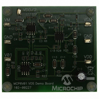
DEMO BOARD FOR MCP6V01
Manufacturer
Microchip Technology
Specifications of MCP6V01DM-VOS
Channels Per Ic
1 - Single
Amplifier Type
Chopper (Zero-Drift)
Output Type
Rail-to-Rail
Slew Rate
0.5 V/µs
Current - Output / Channel
22mA
Operating Temperature
-40°C ~ 125°C
Voltage - Supply, Single/dual (±)
1.8 V ~ 5.5 V
Board Type
Fully Populated
Utilized Ic / Part
MCP6V01
Silicon Manufacturer
Microchip
Application Sub Type
Operational Amplifier
Kit Application Type
Amplifier
Silicon Core Number
MCP6V01, MCP6V03, MCP6V06, MCP6V08
Kit Contents
Board
Lead Free Status / RoHS Status
Lead free / RoHS Compliant
-3db Bandwidth
-
Current - Supply (main Ic)
-
Lead Free Status / Rohs Status
Lead free / RoHS Compliant


MCP6V01 Input Offset Demo Board User’s Guide
1.3
1.4
DS51801A-page 6
INTENDED USE
DESCRIPTION
The MCP6V01 Input Offset Demo Board is intended to provide a simple means to
measure the MCP6V01/2/3 op amp’s input offset voltage (V
conditions. This V
sheet plus changes due to power supply voltage (PSRR), common mode voltage
(CMRR), output voltage (A
Figure 1-2 shows the block diagram for the MCP6V01 Input Offset Demo Board.
FIGURE 1-2:
This circuit does the following:
• Supports Microchip’s auto-zeroed, single op amps:
• Test points for connecting lab equipment
• Single supply configuration
• The bias inputs V
• The V
• The V
• The High Gain Feedback Network and DUT together:
- SOIC-8 package
- Used as both Device Under Test (DUT) and in a difference amplifier
voltage with an op amp in unity gain
- Has a resistor divider at the input that sets V
- When V
- V
- Have a noise gain of G
- Have a common mode gain of 1 V/V
- Produce an output voltage of G
Inputs
open
effect on V
CM
DD
CM
is buffered
/2 Reference uses a resistor ladder to divide V
Reference:
CM
GND
V
V
CM
CM
DD
is driven by an external voltage source, the resistor divider has no
OS
DD
Block Diagram.
includes the specified input offset voltage value found in the data
, V
CM
OL
Reference
Reference
(buffered)
(buffered)
N
and GND set the conditions for the DUT
V
) and temperature (ΔV
≈ 10.0 kV/V
V
DD
CM
/2
N
V
OS
+ V
CM
High Gain
Feedback
Network
Diff. Amp.
DUT
CM
OS
= V
V
/ΔT
DD
REF
DD
A
/2 when that input is left
.
© 2009 Microchip Technology Inc.
).
OS
in half, then buffers that
) under a variety of bias
V
GND
V
DD
V
CM
M
/2
Outputs
Related parts for MCP6V01DM-VOS
Image
Part Number
Description
Manufacturer
Datasheet
Request
R

Part Number:
Description:
IC OPAMP AUTO-ZERO SNGL 8SOIC
Manufacturer:
Microchip Technology
Datasheet:

Part Number:
Description:
300 ?A, Auto-Zeroed Op Amps
Manufacturer:
MICROCHIP [Microchip Technology]
Datasheet:
Part Number:
Description:
Op Amps Sngl Auto-Zero Op Amp E temp
Manufacturer:
Microchip Technology

Part Number:
Description:
300 ?a, Auto-zeroed Op Amps
Manufacturer:
Microchip Technology Inc.
Datasheet:
Part Number:
Description:
Manufacturer:
Microchip Technology Inc.
Datasheet:
Part Number:
Description:
Manufacturer:
Microchip Technology Inc.
Datasheet:
Part Number:
Description:
Manufacturer:
Microchip Technology Inc.
Datasheet:
Part Number:
Description:
Manufacturer:
Microchip Technology Inc.
Datasheet:
Part Number:
Description:
Manufacturer:
Microchip Technology Inc.
Datasheet:
Part Number:
Description:
Manufacturer:
Microchip Technology Inc.
Datasheet:
Part Number:
Description:
Manufacturer:
Microchip Technology Inc.
Datasheet: