NCP690MNADT2GEVB ON Semiconductor, NCP690MNADT2GEVB Datasheet - Page 7
NCP690MNADT2GEVB
Manufacturer Part Number
NCP690MNADT2GEVB
Description
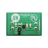
EVAL BOARD FOR NCP690MNADT2G
Manufacturer
ON Semiconductor
Specifications of NCP690MNADT2GEVB
Design Resources
NCP690MNADT2GEVB BOM NCP690MNADT2GEVB Gerber Files NCP690 Demo Brd Schematic
Channels Per Ic
1 - Single
Voltage - Output
1.25 ~ 5 V
Current - Output
1A
Regulator Type
Positive Adjustable
Board Type
Fully Populated
Utilized Ic / Part
NCP690
Lead Free Status / RoHS Status
Lead free / RoHS Compliant
Voltage - Input
-
Operating Temperature
-
Lead Free Status / Rohs Status
Lead free / RoHS Compliant
For Use With/related Products
NCP690MNADT2G
Other names
NCP690MNADT2GEVBOS


Table 6. ELECTRICAL CHARACTERISTICS
values T
Power supply ripple rejection
(Note 8)
Output noise voltage (Note 8)
Thermal Shutdown Temperature
(Note 8)
Thermal Shutdown Hysteresis
(Note 8)
5. Performance guaranteed over the indicated operating temperature range by design and/or characterization tested at T
6. Maximum dropout voltage is limited by minimum input voltage. V
7. Refer to the Applications Information Section.
8. Values based on design and/or characterization.
9. Dropout voltage is defined as the differential voltage between V
1.28
1.27
1.26
1.25
1.24
1.23
1.22
2.55
2.54
2.53
2.52
2.51
2.50
2.49
2.48
2.47
2.46
duty cycle pulse techniques are used during testing to maintain the junction temperature as close to ambient as possible.
current.
−40
−40
J
= 25°C, for Min/Max values T
V
C
Figure 11. Output Voltage vs. Temperature
Figure 13. Output Voltage vs. Temperature
Parameter
IN
IN
−15
−15
= V
= C
OUT_NOM
OUT
T
T
A
A
, AMBIENT TEMPERATURE (°C)
, AMBIENT TEMPERATURE (°C)
= 10 mF
10
10
I
OUT
+ 1 V = 1.75 V,
(V
(V
out
I
35
35
OUT
out
= 1 A
V
C
IN
IN
= 1.25 V)
= 2.5 V)
= 100 mA
= V
= C
I
OUT
V
V
V
BW = 200 Hz to 100 kHz, C
C
J
OUT
IN
PP
I
OUT
60
60
OUT_NOM
OUT
OUT
= −40°C to 125°C; unless otherwise noted. (Note 5) (continued)
= V
= 1 A
= 0.5 V, C
= 1.25 V
= 10 mF, T
= 100 mA
= 10 mF
OUT
85
85
TYPICAL CHARACTERISTICS
+ 1 V, with
+ 1 V = 3.5 V,
Test Conditions
OUT
V
A
IN
= 25°C
110
110
= (V
= 1 mF
http://onsemi.com
OUT
135
135
+ 1 V), V
IN
OUT
IN
7
= 1 mF,
f = 120 Hz
f = 1 kHz
f = 10 kHz
= 1.7 V recommended for guaranteed operation at maximum output
and V
1.55
1.54
1.53
1.52
1.51
1.50
1.49
1.48
1.47
1.46
3.35
3.33
3.31
3.29
3.27
3.25
EN
IN
−40
= V
−40
, when V
IN
Figure 12. Output Voltage vs. Temperature
Figure 14. Output Voltage vs. Temperature
, I
OUT
−15
−15
Symbol
PSRR
OUT
T
T
V
= 1 mA, C
SD
SH
T
N
T
A
A
, AMBIENT TEMPERATURE (°C)
drops 100 mV below its nominal value.
, AMBIENT TEMPERATURE (°C)
10
10
I
OUT
IN
(V
Min
I
(V
OUT
−
−
−
−
−
−
= 10 mF, C
= 1 A
out
35
V
C
35
out
V
C
IN
IN
IN
IN
= 100 mA
= 1.5 V)
= V
= C
= 3.3 V)
= V
= C
OUT_NOM
OUT
60
OUT_NOM
OUT
Typ
60
175
OUT
62
55
40
50
10
= 10 mF
= 10 mF
= 10 mF, for typical
I
OUT
J
85
I
85
OUT
+ 1 V = 2.5 V,
= T
+ 1 V = 4.3 V,
Max
= 100 mA
A
−
−
−
−
−
−
= 1 A
= 25_C. Low
110
110
mV
Unit
dB
°C
°C
135
rms
135
Related parts for NCP690MNADT2GEVB
Image
Part Number
Description
Manufacturer
Datasheet
Request
R

Part Number:
Description:
ON Semiconductor [VOLTAGE REGULATOR]
Manufacturer:
ON Semiconductor
Datasheet:
Part Number:
Description:
357-036-542-201 CARDEDGE 36POS DL .156 BLK LOPRO
Manufacturer:
ON Semiconductor
Datasheet:
Part Number:
Description:
357-036-542-201 CARDEDGE 36POS DL .156 BLK LOPRO
Manufacturer:
ON Semiconductor
Datasheet:
Part Number:
Description:
357-036-542-201 CARDEDGE 36POS DL .156 BLK LOPRO
Manufacturer:
ON Semiconductor
Datasheet:
Part Number:
Description:
357-036-542-201 CARDEDGE 36POS DL .156 BLK LOPRO
Manufacturer:
ON Semiconductor
Datasheet:
Part Number:
Description:
357-036-542-201 CARDEDGE 36POS DL .156 BLK LOPRO
Manufacturer:
ON Semiconductor
Datasheet:
Part Number:
Description:
357-036-542-201 CARDEDGE 36POS DL .156 BLK LOPRO
Manufacturer:
ON Semiconductor
Datasheet:
Part Number:
Description:
357-036-542-201 CARDEDGE 36POS DL .156 BLK LOPRO
Manufacturer:
ON Semiconductor
Datasheet:
Part Number:
Description:
357-036-542-201 CARDEDGE 36POS DL .156 BLK LOPRO
Manufacturer:
ON Semiconductor
Datasheet:
Part Number:
Description:
357-036-542-201 CARDEDGE 36POS DL .156 BLK LOPRO
Manufacturer:
ON Semiconductor
Datasheet:
Part Number:
Description:
357-036-542-201 CARDEDGE 36POS DL .156 BLK LOPRO
Manufacturer:
ON Semiconductor
Datasheet:
Part Number:
Description:
Manufacturer:
ON Semiconductor
Datasheet:
Part Number:
Description:
Manufacturer:
ON Semiconductor
Datasheet:
Part Number:
Description:
Manufacturer:
ON Semiconductor
Datasheet: