NCP690MNADT2GEVB ON Semiconductor, NCP690MNADT2GEVB Datasheet - Page 3
NCP690MNADT2GEVB
Manufacturer Part Number
NCP690MNADT2GEVB
Description
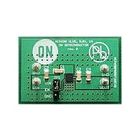
EVAL BOARD FOR NCP690MNADT2G
Manufacturer
ON Semiconductor
Specifications of NCP690MNADT2GEVB
Design Resources
NCP690MNADT2GEVB BOM NCP690MNADT2GEVB Gerber Files NCP690 Demo Brd Schematic
Channels Per Ic
1 - Single
Voltage - Output
1.25 ~ 5 V
Current - Output
1A
Regulator Type
Positive Adjustable
Board Type
Fully Populated
Utilized Ic / Part
NCP690
Lead Free Status / RoHS Status
Lead free / RoHS Compliant
Voltage - Input
-
Operating Temperature
-
Lead Free Status / Rohs Status
Lead free / RoHS Compliant
For Use With/related Products
NCP690MNADT2G
Other names
NCP690MNADT2GEVBOS


Table 1. PIN FUNCTION DESCRIPTION FOR FIXED VERSION
Pin No.
1, 6
GND
GND
GND
2
3
4
5
N/C
EN
EN
IN
IN
IN
Pin Name
GND
OUT
SNS
EN
IN
CURRENT LIMIT
CURRENT LIMIT
CURRENT LIMIT
DRIVER WITH
DRIVER WITH
DRIVER WITH
SHUTDOWN
SHUTDOWN
SHUTDOWN
MOSFET
MOSFET
MOSFET
THERMAL
THERMAL
THERMAL
Voltage inputs which supplies the current to the regulator. Both of these pins should be connected
together for full output current capability
Power supply ground of the regulator. Connected to the die through the lead frame. Soldered to the
copper plane allows for effective heat removal.
For NCP691 and NCP692 this pin functions as Enable Active Low and Enable Active High respect-
ively. For NCP690 this pin has no special meaning and should be left disconnected.
Regulated output voltage
Sense input. This pin should be connected directly to OUT pin.
Figure 5. NCP690 Block Diagram (Fixed Version)
Figure 6. NCP691 Block Diagram (Fixed Version)
Figure 7. NCP692 Block Diagram (Fixed Version)
ENABLE
ENABLE
ENABLE
LOGIC
LOGIC
LOGIC
http://onsemi.com
3
REFERENCE
REFERENCE
REFERENCE
BANDGAP
BANDGAP
BANDGAP
Description
R1
R1
R1
DISCHARGE
DISCHARGE
DISCHARGE
ACTIVE
ACTIVE
ACTIVE
R2
R2
R2
SNS
SNS
OUT
OUT
OUT
SNS
Related parts for NCP690MNADT2GEVB
Image
Part Number
Description
Manufacturer
Datasheet
Request
R

Part Number:
Description:
ON Semiconductor [VOLTAGE REGULATOR]
Manufacturer:
ON Semiconductor
Datasheet:
Part Number:
Description:
357-036-542-201 CARDEDGE 36POS DL .156 BLK LOPRO
Manufacturer:
ON Semiconductor
Datasheet:
Part Number:
Description:
357-036-542-201 CARDEDGE 36POS DL .156 BLK LOPRO
Manufacturer:
ON Semiconductor
Datasheet:
Part Number:
Description:
357-036-542-201 CARDEDGE 36POS DL .156 BLK LOPRO
Manufacturer:
ON Semiconductor
Datasheet:
Part Number:
Description:
357-036-542-201 CARDEDGE 36POS DL .156 BLK LOPRO
Manufacturer:
ON Semiconductor
Datasheet:
Part Number:
Description:
357-036-542-201 CARDEDGE 36POS DL .156 BLK LOPRO
Manufacturer:
ON Semiconductor
Datasheet:
Part Number:
Description:
357-036-542-201 CARDEDGE 36POS DL .156 BLK LOPRO
Manufacturer:
ON Semiconductor
Datasheet:
Part Number:
Description:
357-036-542-201 CARDEDGE 36POS DL .156 BLK LOPRO
Manufacturer:
ON Semiconductor
Datasheet:
Part Number:
Description:
357-036-542-201 CARDEDGE 36POS DL .156 BLK LOPRO
Manufacturer:
ON Semiconductor
Datasheet:
Part Number:
Description:
357-036-542-201 CARDEDGE 36POS DL .156 BLK LOPRO
Manufacturer:
ON Semiconductor
Datasheet:
Part Number:
Description:
357-036-542-201 CARDEDGE 36POS DL .156 BLK LOPRO
Manufacturer:
ON Semiconductor
Datasheet:
Part Number:
Description:
Manufacturer:
ON Semiconductor
Datasheet:
Part Number:
Description:
Manufacturer:
ON Semiconductor
Datasheet:
Part Number:
Description:
Manufacturer:
ON Semiconductor
Datasheet: