IRPLLED1 International Rectifier, IRPLLED1 Datasheet - Page 25
IRPLLED1
Manufacturer Part Number
IRPLLED1
Description
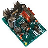
BOARD EVALUATION FOR IRS2540PBF
Manufacturer
International Rectifier
Specifications of IRPLLED1
Current - Output / Channel
1.5A
Outputs And Type
1, Non-Isolated
Voltage - Output
24V
Features
Dimmable
Voltage - Input
50 ~ 170V
Utilized Ic / Part
IRS2540PBF
Core Chip
IRS2540, IRS2541, IRS25401
Topology
Buck (Step Down)
No. Of Outputs
1
Output Current
1.5A
Output Voltage
500mV
Dimming Control Type
PWM
Development Tool Type
Hardware - Eval/Demo Board
Lead Free Status / RoHS Status
Contains lead / RoHS compliant by exemption


Filtering
The RC filter at the IFB pin is used to remove high frequency transients associated with the switching. The corner
frequency of this filter was left high enough to prevent any further distortion of the feedback signal.
The input filter is a low-pass filter. Its main objective is to prevent ringing of comparable frequency on Vbus. Exact
values of capacitance and inductance are not of critical importance, so long as adequate filtering is accomplished. In
addition to the electrolytic capacitor that is used for filtering on the bus there is also a small ceramic for decoupling
of high frequency noise. Ceramic capacitors typically have low ESR such that they are more ideal for high
frequency filtering.
The IRS2540/1/01/11 was specifically designed to handle low frequency ripples on VBUS. Its capability to handle
such ripple makes it ideal for an offline rectified waveform. However if high voltage (on the order of 5V-10V) high
frequency oscillations (greater than or close to the operating frequency) are present on VBUS, it is recommended to
implement an input filter. If these high frequency signals are present on VBUS the IRS2540/1/01/11 will still
continue to regulate the current through the load, however abnormal switching of LO and HO may be observed.
This poses a problem in terms of switching losses. As previously discussed, the application may need to control the
operating frequency to optimize the system efficiency. Excessive high frequency ripple at the DC bus could cause
the frequency to become unstable, since this system relies on a self-oscillating principle and is sensitive to noise.
Careful attention to the PCB layout is also necessary for this system to operate correctly. If filters on IFB and VCC
are not placed correctly, high frequency ripple will couple to the IFB input and interfere with the operation of the
control loop. Also if the load current is 1A or 1.5A, when HO turns on the load immediately tries to draw this
current. Since the circuit supply is not usually close by, the capacitance of the input wire is not enough to
compensate for this large pull of current and this can result in oscillations or change in potential on the input line.
To alleviate the circuit of such potential problems it is advisable to implement an input filter. The input filter will
also greatly improve the EMC performance.
EMC performance
The IRPLLED1 evaluation board has not been EMC tested. Input and Output filters can be used to reduce the
conducted emissions to below the limits of the applicable EMC standard as needed. Inductors may require a
powdered Iron core rather than Ferrite, which can handle a much larger current before saturating. If EMC is of
critical importance, it may be beneficial to use a MOSFET for the upper switching element and a diode for the
lower switch. The reverse recovery time for a diode is inherently shorter than that of a MOSFET and this can help
in reducing transients observed in the switching elements resulting in better EMC performance.
Layout Considerations
It is very important when laying out the PCB for the IRS2540/1/01/11 based ballast to consider the following points:
www.irf.com
10. Other Design Considerations
1. CVCC2 and CF must be as close to IC1 as possible.
2. The feedback path should be kept to a minimum without crossing any high frequency lines.
3. COUT should be as close to the main inductor as possible.
4. All traces that form the nodes VS and VB should be kept as short as possible.
5. It is essential that all signal and power grounds should be kept separated from each other to prevent noise
from entering the control environment. Signal and power grounds should be connected together at one point
only, which must be at the COM pin of the IRS2540/1/01/11. The IRS2540/1/01/11 is very sensitive to noise
and will not operate if these guidelines are not followed!
RD-0608
25
Related parts for IRPLLED1
Image
Part Number
Description
Manufacturer
Datasheet
Request
R

Part Number:
Description:
SCHOTTKY RECTIFIER
Manufacturer:
International Rectifier Corp.
Datasheet:
Part Number:
Description:
SCHOTTKY RECTIFIER
Manufacturer:
International Rectifier Corp.
Datasheet:
Part Number:
Description:
SCHOTTKY RECTIFIER
Manufacturer:
International Rectifier Corp.
Datasheet:
Part Number:
Description:
SCHOTTKY RECTIFIER
Manufacturer:
International Rectifier Corp.
Datasheet:
Part Number:
Description:
SCHOTTKY RECTIFIER
Manufacturer:
International Rectifier Corp.
Datasheet:
Part Number:
Description:
SCHOTTKY RECTIFIER
Manufacturer:
International Rectifier Corp.
Datasheet:
Part Number:
Description:
SCHOTTKY RECTIFIER
Manufacturer:
International Rectifier Corp.
Datasheet:
Part Number:
Description:
SCHOTTKY RECTIFIER
Manufacturer:
International Rectifier Corp.
Datasheet:
Part Number:
Description:
SCHOTTKY RECTIFIER
Manufacturer:
International Rectifier Corp.
Datasheet:
Part Number:
Description:
SCHOTTKY RECTIFIER
Manufacturer:
International Rectifier Corp.
Datasheet:
Part Number:
Description:
SCHOTTKY RECTIFIER
Manufacturer:
International Rectifier Corp.
Datasheet:
Part Number:
Description:
SCHOTTKY RECTIFIER
Manufacturer:
International Rectifier Corp.
Datasheet:
Part Number:
Description:
SCHOTTKY RECTIFIER
Manufacturer:
International Rectifier Corp.
Datasheet:
Part Number:
Description:
SCHOTTKY RECTIFIER
Manufacturer:
International Rectifier Corp.
Datasheet:
Part Number:
Description:
SCHOTTKY RECTIFIER
Manufacturer:
International Rectifier Corp.
Datasheet: