STEVAL-ILL027V1 STMicroelectronics, STEVAL-ILL027V1 Datasheet - Page 7
STEVAL-ILL027V1
Manufacturer Part Number
STEVAL-ILL027V1
Description
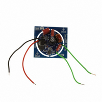
BOARD EVAL LED DRIVER FOR L6562A
Manufacturer
STMicroelectronics
Datasheets
1.L6562ADTR.pdf
(26 pages)
2.STEVAL-ILL027V1.pdf
(4 pages)
3.STEVAL-ILL027V1.pdf
(23 pages)
Specifications of STEVAL-ILL027V1
Design Resources
STEVAL-ILL027V1 Schematics STEVAL-ILL027V1 BOM STEVAL-ILL027V1 Gerber Files
Current - Output / Channel
260mA
Outputs And Type
1, Non-Isolated
Voltage - Output
70V
Features
Short-Circuit Protection
Voltage - Input
120VAC
Utilized Ic / Part
L6562A
Product
Display Modules
Lead Free Status / RoHS Status
Lead free by exemption / RoHS compliant by exemption
Other names
497-10170


AN3111
The proposed circuit runs at constant peak current. The current sensing voltage is set for 1
V, which is the clamping voltage of the current sensing comparator of the L6562A. The
voltage of the LED string is sensed on the INV pin of the L6562A through a coupled winding.
The turn ratio of the coupled inductor is designed so that the feedback voltage is lower than
2.5 V in normal operating conditions, so the error amplifier is saturated at maximum level
which sets the max. current sensing voltage to 1 V. Therefore, the peak current of the
inductor is fixed at a level determined by the sensing resistor value. As the peak current of
the inductor is constant, the input power is constant. The LED voltage is considered
constant, and the current into the LED can also be considered constant. If the load (the
LEDs) is open, the reflected output voltage on the INV pin is above a certain level, and the
controller shuts down to provide open load protection.
If the inductor current is controlled at constant level all the time, then the power factor is very
poor. The multiplier of the L6562A is used to reshape the current amplitude near the line
voltage zero crossing to improve the power factor. The rectified sine waveform is sampled at
the MULT pin. The output of the multiplier, which is the current setting, is lower than setting
the level near the line voltage zero crossing. In this way, the power factor of the converter is
improved significantly.
Design procedure:
●
●
●
The design variable is the peak current of the inductor (Ipk), and the inductance (L).
When Q1 is turned on, the inductor is charged to Ipk. The ON time is:
Equation 1
The OFF time is:
Equation 2
The period of the switching cycle is:
Equation 3
The duty cycle (D) is:
Equation 4
Input voltage:
Output voltage: 18 LEDs in series, Vout=54 V
Output current: Iout=350 mA
Vin θ ( )
=
( T
θ
2
)
Doc ID 16815 Rev 2
⋅
=
( D
Vin
Ton
θ
)
=
⋅
(
θ
Ton
Toff
Ton
sin
)
( T
+
θ ( )
Toff
θ
(
(
(
)
θ
θ
θ
,
Vin
)
)
)
=
=
(
=
θ
L
)
L
Vout
=
Vin
Vout
=
*
*
120V
Ipk
Ipk
L
Vin
) t (
Vout
*
+
Ipk
(
Vin
θ
)
+
(
θ
L
)
Vout
*
Ipk
Circuit design
7/23
Related parts for STEVAL-ILL027V1
Image
Part Number
Description
Manufacturer
Datasheet
Request
R

Part Number:
Description:
BOARD EVAL FOR MEMS SENSORS
Manufacturer:
STMicroelectronics
Datasheet:

Part Number:
Description:
KIT DEV STARTER ST10F276Z5
Manufacturer:
STMicroelectronics
Datasheet:

Part Number:
Description:
BOARD EVAL HDMI $ VIDEO SWITCH
Manufacturer:
STMicroelectronics
Datasheet:

Part Number:
Description:
BOARD DEMO ACCELEROMETER DIL24
Manufacturer:
STMicroelectronics
Datasheet:

Part Number:
Description:
BOARD STLM75/STDS75/ST72F651
Manufacturer:
STMicroelectronics
Datasheet:

Part Number:
Description:
EVAL BOARD 3AXIS MEMS ACCELLRMTR
Manufacturer:
STMicroelectronics
Datasheet:

Part Number:
Description:
BOARD EVAL 8BIT MICRO + TDE1708
Manufacturer:
STMicroelectronics
Datasheet:

Part Number:
Description:
EVAL BOARD A/D TS4657
Manufacturer:
STMicroelectronics
Datasheet:

Part Number:
Description:
BOARD ADAPTER 20DIP LIS3LV02DL
Manufacturer:
STMicroelectronics
Datasheet:

Part Number:
Description:
BOARD DEMO STM8S207R6/LIS331DLH
Manufacturer:
STMicroelectronics
Datasheet:

Part Number:
Description:
STMicroelectronics [RIPPLE-CARRY BINARY COUNTER/DIVIDERS]
Manufacturer:
STMicroelectronics
Datasheet:
Part Number:
Description:
STMicroelectronics [LIQUID-CRYSTAL DISPLAY DRIVERS]
Manufacturer:
STMicroelectronics
Datasheet:
Part Number:
Description:
BOARD EVAL FOR MEMS SENSORS
Manufacturer:
STMicroelectronics
Datasheet: