NCP5602EVB ON Semiconductor, NCP5602EVB Datasheet - Page 6
NCP5602EVB
Manufacturer Part Number
NCP5602EVB
Description
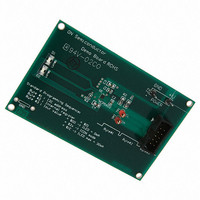
EVAL BOARD FOR NCP5602
Manufacturer
ON Semiconductor
Specifications of NCP5602EVB
Design Resources
NCP5602 EVB BOM NCP5602EVB Gerber Files NCP5602 EVB Schematic
Current - Output / Channel
60mA
Outputs And Type
2, Non-Isolated
Voltage - Output
4.8 ~ 5.7 V
Features
Dimmable
Voltage - Input
3.6V
Utilized Ic / Part
NCP5602
Core Chip
NCP5602
Topology
Charge Pump
No. Of Outputs
2
Development Tool Type
Hardware - Eval/Demo Board
Leaded Process Compatible
Yes
Mcu Supported Families
NCP5602
Rohs Compliant
Yes
Lead Free Status / RoHS Status
Lead free / RoHS Compliant
For Use With/related Products
NCP5602
Other names
NCP5602EVBOS


DC−DC Operation
generate a DC voltage capable to supply the White LED
load. The system regulates the current flowing into each
LED by means of internal current mirrors associated with
the white diodes. Consequently, the output voltage will be
equal to the Vf of the LED, plus the drop voltage (ranging
from 200 mV to 400 mV, depending upon the output
current) developed across the internal NMOS mirror.
Typically, assuming a standard white LED forward biased
at 10 mA, the output voltage will be 3.8 V.
output and stops the converter when the voltage is above
5.0 V. The converter resumes to normal operation when the
voltage drops below 5.0 V (no latchup mechanism).
Consequently, the chip can operate with no load during any
test procedures.
Load Current Calculation
voltage provided by the internal Bandgap associated to the
external resistor connected across I
Figure 3). In any case, no voltage shall be forced at I
pin, either downward or upward.
k = 500 to yield the output load current. Since the reference
voltage is based on a temperature compensated Bandgap,
a tight tolerance resistor will provide a very accurate load
current. The resistor is calculated from the Ohm’s law
(R
arranged to define the resistor value for a given output
current:
The converter is based on a charge pump technique to
The built−in OVP circuit continuously monitor each
The load current is derived from the 600 mV reference
The reference current is multiplied by the constant
bias
= Vref/I
REF
R bias + (Vref * k) Iout
R bias + (0.6 * 500) Iout
) and a more practical equation can be
7
2
3
Figure 4. Typical Single and Double LED Connections
REF
pin and Ground (see
GND
APPLICATION INFORMATION
http://onsemi.com
(eq. 1)
REF
6
R
600 kW. Obviously, the tolerance of such a resistor must be
1% or better, with a 100 ppm thermal coefficient, to get the
expected overall tolerance.
Load Connection
simultaneously, as depicted in Figure 1, but the load can be
arranged to accommodate one or two LED if necessary in
the application (see Figure 4). In this case, the two current
mirrors can be connected in parallel to drive a single power
full LED, thus yielding 60 mA current capability in a single
LED.
GND
bias
Consequently, the resistor value will range between
The NCP5602 chip is capable to drive the two LED
R1
I
= 300/30 mA = 10 kW and R
REF
7
2
3
Figure 3. Basic Reference Current Source
Pin 4
VBandgap
+
-
Note: The I
biased by an external voltage.
R bias + 300 Iout
600mV
REF
pin must never be
GND
bias
= 300/0.5 mA =
GND
LED Return
Pin 2 & 3
(eq. 2)
Related parts for NCP5602EVB
Image
Part Number
Description
Manufacturer
Datasheet
Request
R

Part Number:
Description:
High Efficiency Ultra Small Thinnest White LED Driver
Manufacturer:
ON Semiconductor
Datasheet:
Part Number:
Description:
ON Semiconductor [VOLTAGE REGULATOR]
Manufacturer:
ON Semiconductor
Datasheet:
Part Number:
Description:
357-036-542-201 CARDEDGE 36POS DL .156 BLK LOPRO
Manufacturer:
ON Semiconductor
Datasheet:
Part Number:
Description:
357-036-542-201 CARDEDGE 36POS DL .156 BLK LOPRO
Manufacturer:
ON Semiconductor
Datasheet:
Part Number:
Description:
357-036-542-201 CARDEDGE 36POS DL .156 BLK LOPRO
Manufacturer:
ON Semiconductor
Datasheet:
Part Number:
Description:
357-036-542-201 CARDEDGE 36POS DL .156 BLK LOPRO
Manufacturer:
ON Semiconductor
Datasheet:
Part Number:
Description:
357-036-542-201 CARDEDGE 36POS DL .156 BLK LOPRO
Manufacturer:
ON Semiconductor
Datasheet:
Part Number:
Description:
357-036-542-201 CARDEDGE 36POS DL .156 BLK LOPRO
Manufacturer:
ON Semiconductor
Datasheet:
Part Number:
Description:
357-036-542-201 CARDEDGE 36POS DL .156 BLK LOPRO
Manufacturer:
ON Semiconductor
Datasheet:
Part Number:
Description:
357-036-542-201 CARDEDGE 36POS DL .156 BLK LOPRO
Manufacturer:
ON Semiconductor
Datasheet:
Part Number:
Description:
357-036-542-201 CARDEDGE 36POS DL .156 BLK LOPRO
Manufacturer:
ON Semiconductor
Datasheet:
Part Number:
Description:
357-036-542-201 CARDEDGE 36POS DL .156 BLK LOPRO
Manufacturer:
ON Semiconductor
Datasheet:
Part Number:
Description:
Manufacturer:
ON Semiconductor
Datasheet:
Part Number:
Description:
Manufacturer:
ON Semiconductor
Datasheet: