MCP4728EV Microchip Technology, MCP4728EV Datasheet - Page 47
MCP4728EV
Manufacturer Part Number
MCP4728EV
Description
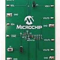
BOARD EVAL 12BIT 4CH DAC MCP4728
Manufacturer
Microchip Technology
Type
D/Ar
Specifications of MCP4728EV
Number Of Dac's
4
Number Of Bits
12
Outputs And Type
1, Single Ended
Data Interface
I²C
Settling Time
6µs
Dac Type
Voltage
Voltage Supply Source
Single
Operating Temperature
-40°C ~ 125°C
Utilized Ic / Part
MCP4728
Product
Data Conversion Development Tools
Resolution
12 bit
Interface Type
I2C
Supply Voltage (max)
5.5 V
Supply Voltage (min)
2.7 V
Silicon Manufacturer
Microchip
Silicon Core Number
MCP4728
Kit Application Type
Data Converter
Application Sub Type
DAC
Kit Contents
Board
For Use With/related Products
MCP4728
Lead Free Status / RoHS Status
Lead free / RoHS Compliant
Lead Free Status / RoHS Status
Lead free / RoHS Compliant, Lead free / RoHS Compliant
Available stocks
Company
Part Number
Manufacturer
Quantity
Price
Company:

Part Number:
MCP4728EV
Manufacturer:
Microchip Technology
Quantity:
135
Company:
Part Number:
MCP4728EV
Manufacturer:
MICROCHIP
Quantity:
12 000


C.1
TABLE C-1:
© 2009 Microchip Technology Inc.
Fast Mode Write
Write DAC Input Register and EEPROM
Write I
Note 1:
Command Field
C2
0
0
0
2:
3:
4:
2
C1
C Address Bits (A2, A1, A0)
0
1
INTRODUCTION
1
The analog output is updated when LDAC pin is (or changes to) “Low”. UDAC bit is not used for this
command.
The DAC output is updated when LDAC pin or UDAC bit is “Low”.
The device starts writing to the EEPROM on the acknowledge clock pulse of the last channel. The device
does not execute any command until RDY/BSY bit comes back to “High”.
The input and output registers are updated at the acknowledge clock pulse of the last byte. The update
does not require LDAC pin or UDAC bit conditions. EEPROM is not affected.
Appendix C. MCP4728 Read/Write Commands
C0
X
0
1
WRITE COMMAND TYPES
Function
W1
Not Used
Not Used
0
1
1
Write
Table summarizes the write command types and their functions. The write command
is defined by using three write command type bits (C2, C1, C0) and two write function
bits (W1, W0). Writing and reading the I
PICKit Serial Analyzer. Please see the MCP4728 data sheet for more details on the
commands.
W0
0
0
1
Sequential Write for
DAC Input Regis-
ters and EEPROM
Multi-Write for DAC
DAC Input Register
Fast Write for DAC
Write I
Command Name
Single Write for
Input Registers
Input Registers
and EEPROM
2
Bits
C Address
MCP4728 EVALUATION BOARD
This command writes to the DAC input registers sequentially
with limited configuration bits. The data is sent sequentially
from channels A to D. The input register is written at the
acknowledge clock pulse of the channel’s last input data byte.
EEPROM is not affected. (Note 1)
This command writes to multiple DAC input registers, one DAC
input register at a time. The writing channel register is defined
by the DAC selection bits (DAC1, DAC0). EEPROM is not
affected. (Note 2)
This command writes to both the DAC input registers and
EEPROM sequentially. The sequential writing is carried out
from a starting channel to channel D. The starting channel is
defined by the DAC selection bits (DAC1 and DAC0).
The input register is written at the acknowledge clock pulse of
the last input data byte of each register. However, the
EEPROM data is written altogether at the same time sequen-
tially at the end of the last byte. (Note 2),(Note 3)
This command writes to a single selected DAC input register
and its EEPROM. Both the input register and EEPROM are
written at the acknowledge clock pulse of the last input data
byte. The writing channel is defined by the DAC selection bits
(DAC1 and
This command writes new I
DAC input register and EEPROM.
DAC0).
2
C address bits are not demonstrated with the
(Note 2),(Note 3)
Function
2
C address bits (A2, A1, A0) to the
USER’S GUIDE
DS51837A-page 43
Related parts for MCP4728EV
Image
Part Number
Description
Manufacturer
Datasheet
Request
R

Part Number:
Description:
Manufacturer:
Microchip Technology Inc.
Datasheet:
Part Number:
Description:
Manufacturer:
Microchip Technology Inc.
Datasheet:
Part Number:
Description:
Manufacturer:
Microchip Technology Inc.
Datasheet:
Part Number:
Description:
Manufacturer:
Microchip Technology Inc.
Datasheet:
Part Number:
Description:
Manufacturer:
Microchip Technology Inc.
Datasheet:
Part Number:
Description:
Manufacturer:
Microchip Technology Inc.
Datasheet:
Part Number:
Description:
Manufacturer:
Microchip Technology Inc.
Datasheet:
Part Number:
Description:
Manufacturer:
Microchip Technology Inc.
Datasheet: