SI3461-KIT Silicon Laboratories Inc, SI3461-KIT Datasheet - Page 16
SI3461-KIT
Manufacturer Part Number
SI3461-KIT
Description
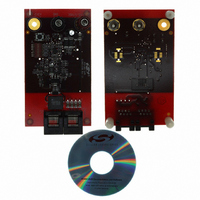
BOARD EVAL FOR SI3461
Manufacturer
Silicon Laboratories Inc
Type
Controllers & Processorsr
Specifications of SI3461-KIT
Main Purpose
Special Purpose DC/DC, Power Over Ethernet
Board Type
Fully Populated
Utilized Ic / Part
Si3461
Ethernet Connection Type
10/100 Base-T, IEEE 802.3
Interface Type
Ethernet
Operating Voltage
12 V to 15 V
Operating Current
10 mA
Product
Modules
For Use With/related Products
Si3460
Lead Free Status / RoHS Status
Lead free / RoHS non-compliant
Current - Output
-
Voltage - Output
-
Voltage - Input
-
Power - Output
-
Frequency - Switching
-
Outputs And Type
-
Regulator Topology
-
Lead Free Status / Rohs Status
Lead free / RoHS Compliant
Other names
336-1843


Si3461
7. Si3461 Pin Descriptions
Si3461 pin functionality is described in Table 7. Note that the information applies to the Si3461 device pins, while
the Si3461-EVB User's Guide describes the inputs and outputs of the evaluation system.
Refer to the complete Si3461-EVB schematics and BOM listing for information about the external components
needed for the complete PSE application circuit.
16
Pin #
1
2
3
4
5
6
7
8
9
CLSMODE
CLSMARK
Pin Name
VSENSE
ISENSE
DETA
VDD
DC1
DC2
RST
Digital output
Digital output
Digital output
Digital output
Analog input
Analog input
Analog input
Digital input
Pin Type
Power
CLSMODE
CLSMARK
Table 7. Si3461 Pin Functionality
VDD
DC1
DC2
Top View—Pads on bottom of package
1
2
3
4
5
Logic high on this output increases the current capability of the
detection circuitry while used for mark pulse generation. Refer to
the Si3461-EVB schematics.
This is a PWM output providing the dc control voltage for the
detection circuitry. It is also combined with the DC2 output in a
ratio of 1:256 to provide the gate control voltage of the pass FET.
3.3 V power supply input.
This is a PWM output that (combined with the DC1 output) pro-
vides the gate control voltage of the pass FET with high resolution.
This is an open drain output. When high, it enables the feedback
path controlling the 18 V classification voltage.
DETA is an analog input pin. During the detection process, the
DC1 pin duty cycle is varied to generate filtered dc voltages
across the load, and the voltage drop across a current sensing
resistor is measured through the DETA input.
VSENSE is an analog input used for sensing the input dc voltage.
Active low reset input. When low, it places the Si3461 device into
an inactive state. When pulled high, the device begins the detec-
tion process sequence.
ISENSE is an analog input connected to a current sense resistor
for output current sensing.
11-pin QFN (3x3 mm)
Rev. 1.0
Si3461
GND
10
9
8
7
6
STATUS
ISENSE
RST
VSENSE
DETA
Pin Function
Related parts for SI3461-KIT
Image
Part Number
Description
Manufacturer
Datasheet
Request
R

Part Number:
Description:
QFN 11/I°/SINGLE-PORT POE / POE+ PSE INTERFACE
Manufacturer:
Silicon Laboratories Inc
Part Number:
Description:
IC POWER MANAGEMENT CTLR 11VQFN
Manufacturer:
Silicon Laboratories Inc
Datasheet:
Part Number:
Description:
IC POWER MANAGEMENT CTLR 11VQFN
Manufacturer:
Silicon Laboratories Inc
Datasheet:
Part Number:
Description:
IC POWER MANAGEMENT CTLR 11VQFN
Manufacturer:
Silicon Laboratories Inc
Datasheet:
Part Number:
Description:
SMD/C°/SINGLE-ENDED OUTPUT SILICON OSCILLATOR
Manufacturer:
Silicon Laboratories Inc
Part Number:
Description:
Manufacturer:
Silicon Laboratories Inc
Datasheet:
Part Number:
Description:
N/A N/A/SI4010 AES KEYFOB DEMO WITH LCD RX
Manufacturer:
Silicon Laboratories Inc
Datasheet:
Part Number:
Description:
N/A N/A/SI4010 SIMPLIFIED KEY FOB DEMO WITH LED RX
Manufacturer:
Silicon Laboratories Inc
Datasheet:
Part Number:
Description:
N/A/-40 TO 85 OC/EZLINK MODULE; F930/4432 HIGH BAND (REV E/B1)
Manufacturer:
Silicon Laboratories Inc
Part Number:
Description:
EZLink Module; F930/4432 Low Band (rev e/B1)
Manufacturer:
Silicon Laboratories Inc
Part Number:
Description:
I°/4460 10 DBM RADIO TEST CARD 434 MHZ
Manufacturer:
Silicon Laboratories Inc
Part Number:
Description:
I°/4461 14 DBM RADIO TEST CARD 868 MHZ
Manufacturer:
Silicon Laboratories Inc
Part Number:
Description:
I°/4463 20 DBM RFSWITCH RADIO TEST CARD 460 MHZ
Manufacturer:
Silicon Laboratories Inc
Part Number:
Description:
I°/4463 20 DBM RADIO TEST CARD 868 MHZ
Manufacturer:
Silicon Laboratories Inc