LM25574EVAL National Semiconductor, LM25574EVAL Datasheet - Page 17
LM25574EVAL
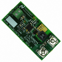
Manufacturer Part Number
LM25574EVAL
Description
BOARD EVALUATION FOR LM25574
Manufacturer
National Semiconductor
Series
PowerWise®, SIMPLE SWITCHER®r
Specifications of LM25574EVAL
Main Purpose
DC/DC, Step Down
Outputs And Type
1, Non-Isolated
Voltage - Output
5V
Current - Output
500mA
Voltage - Input
7 ~ 42V
Regulator Topology
Buck
Frequency - Switching
300kHz
Board Type
Fully Populated
Utilized Ic / Part
LM25574
Lead Free Status / RoHS Status
Not applicable / Not applicable
Power - Output
-
Other names
*LM25574EVAL


PCB LAYOUT AND THERMAL CONSIDERATIONS
The circuit in Figure 1 serves as both a block diagram of the
LM25574 and a typical application board schematic for the
LM25574. In a buck regulator there are two loops where cur-
rents are switched very fast. The first loop starts from the input
capacitors, to the regulator VIN pin, to the regulator SW pin,
to the inductor then out to the load. The second loop starts
from the output capacitor ground, to the regulator PGND pins,
to the regulator IS pins, to the diode anode, to the inductor
and then out to the load. Minimizing the loop area of these
two loops reduces the stray inductance and minimizes noise
and possible erratic operation. A ground plane in the PC
board is recommended as a means to connect the input filter
capacitors to the output filter capacitors and the PGND pins
of the regulator. Connect all of the low power ground connec-
tions (C
Connect the AGND and PGND pins together through the top-
side copper trace. Place several vias in this trace to the
ground plane.
The two highest power dissipating components are the re-
circulating diode and the LM25574 regulator IC. The easiest
method to determine the power dissipated within the
LM25574 is to measure the total conversion losses (Pin –
Pout) then subtract the power losses in the Schottky diode,
output inductor and snubber resistor. An approximation for
the Schottky diode loss is P = (1-D) x Iout x Vfwd. An approx-
imation for the output inductor power is P = I
SS
, R
T
, C
RAMP
) directly to the regulator AGND pin.
OUT
2
x R x 1.1,
17
where R is the DC resistance of the inductor and the 1.1 factor
is an approximation for the AC losses. If a snubber is used,
an approximation for the damping resistor power dissipation
is P = Vin
quency and Csnub is the snubber capacitor.
The most significant variables that affect the power dissipated
by the LM25574 are the output current, input voltage and op-
erating frequency. The power dissipated while operating near
the maximum output current and maximum input volatge can
be appreciable. The operating frequency of the LM25574
evaluation board has been designed for 300kHz. When op-
erating at 0.5A output current with a 42V input the power
dissipation of the LM25574 regulator is approximately 0.36W.
The junction-to-ambient thermal resistance of the LM25574
will vary with the application. The most significant variables
are the area of copper in the PC board, and the amount of
forced air cooling provided. The junction-to-ambient thermal
resistance of the LM25574 mounted in the evaluation board
varies from 90°C/W with no airflow to 60°C/W with 900 LFM
(Linear Feet per Minute). With a 25°C ambient temperature
and no airflow, the predicted junction temperature for the
LM25574 will be 25 + ((90 x 0.36) = 57°C. If the evaluation
board is operated at 0.5A output current, 42V input voltage
and high ambient temperature for a prolonged period of time
the thermal shutdown protection within the IC may activate.
The IC will turn off allowing the junction to cool, followed by
restart with the soft-start capacitor reset to zero.
2
x Fsw x Csnub, where Fsw is the switching fre-
www.national.com
Related parts for LM25574EVAL
Image
Part Number
Description
Manufacturer
Datasheet
Request
R

Part Number:
Description:
National Semiconductor [8-Bit D/A Converter]
Manufacturer:
National Semiconductor
Datasheet:
Part Number:
Description:
National Semiconductor [Media Coprocessor]
Manufacturer:
National Semiconductor
Datasheet:
Part Number:
Description:
Digitally Controlled Tone and Volume Circuit with Stereo Audio Power Amplifier, Microphone Preamp Stage and National 3D Sound
Manufacturer:
National Semiconductor
Datasheet:
Part Number:
Description:
Digitally Controlled Tone and Volume Circuit with Stereo Audio Power Amplifier, Microphone Preamp Stage and National 3D Sound
Manufacturer:
National Semiconductor
Datasheet:
Part Number:
Description:
AC97 Rev 2 Codec with Sample Rate Conversion and National 3D Sound
Manufacturer:
National Semiconductor
Part Number:
Description:
Manufacturer:
National Semiconductor
Datasheet:
Part Number:
Description:
Manufacturer:
National Semiconductor
Datasheet:
Part Number:
Description:
General Purpose, Low Voltage, Low Power, Rail-to-Rail Output Operational Amplifiers
Manufacturer:
National Semiconductor
Datasheet:
Part Number:
Description:
8-bit 20 MSPS flash A/D converter.
Manufacturer:
National Semiconductor
Datasheet:
Part Number:
Description:
Low Noise Quad Operational Amplifier
Manufacturer:
National Semiconductor
Datasheet:
Part Number:
Description:
Quad Differential Line Receivers
Manufacturer:
National Semiconductor
Datasheet:
Part Number:
Description:
Quad High Speed Trapezoidal? Bus Transceiver
Manufacturer:
National Semiconductor
Datasheet:
Part Number:
Description:
Dual Line Receiver
Manufacturer:
National Semiconductor
Datasheet:
Part Number:
Description:
TTL to 10k ECL Level Translator with Latch
Manufacturer:
National Semiconductor
Datasheet: