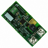
LM25574EVAL National Semiconductor, LM25574EVAL Datasheet - Page 14

LM25574EVAL
Manufacturer Part Number
LM25574EVAL
Description
BOARD EVALUATION FOR LM25574
Manufacturer
National Semiconductor
Series
PowerWise®, SIMPLE SWITCHER®r
Specifications of LM25574EVAL
Main Purpose
DC/DC, Step Down
Outputs And Type
1, Non-Isolated
Voltage - Output
5V
Current - Output
500mA
Voltage - Input
7 ~ 42V
Regulator Topology
Buck
Frequency - Switching
300kHz
Board Type
Fully Populated
Utilized Ic / Part
LM25574
Lead Free Status / RoHS Status
Not applicable / Not applicable
Power - Output
-
Other names
*LM25574EVAL
www.national.com
minimum ripple voltage. A good approximation for the re-
quired ripple current rating necessary is I
Quality ceramic capacitors with a low ESR should be selected
for the input filter. To allow for capacitor tolerances and volt-
age effects, one 1.0µF, 100V ceramic capacitor will be used.
If step input voltage transients are expected near the maxi-
mum rating of the LM25574, a careful evaluation of ringing
and possible spikes at the device VIN pin should be complet-
ed. An additional damping network or input voltage clamp
may be required in these cases.
C8
The capacitor at the VCC pin provides noise filtering and sta-
bility for the V
should be no smaller than 0.1µF, and should be a good qual-
ity, low ESR, ceramic capacitor. A value of 0.47µF was se-
lected for this design.
C7
The bootstrap capacitor between the BST and the SW pins
supplies the gate current to charge the buck switch gate at
turn-on. The recommended value of C7 is 0.022µF, and
should be a good quality, low ESR, ceramic capacitor.
C4
The capacitor at the SS pin determines the soft-start time, i.e.
the time for the reference voltage and the output voltage, to
reach the final regulated value. The time is determined from:
For this application, a C4 value of 0.01µF was chosen which
corresponds to a soft-start time of 1ms.
R5, R6
R5 and R6 set the output voltage level, the ratio of these re-
sistors is calculated from:
For a 5V output, the R5/R6 ratio calculates to 3.082. The re-
sistors should be chosen from standard value resistors, a
good starting point is selection in the range of 1.0kΩ - 10kΩ.
Values of 5.11kΩ for R5, and 1.65kΩ for R6 were selected.
R1, R2, C2
A voltage divider can be connected to the SD pin to set a
minimum operating voltage Vin
feature is required, the easiest approach to select the divider
resistor values is to select a value for R1 (between 10kΩ and
100kΩ recommended) then calculate R2 from:
Capacitor C2 provides filtering for the divider. The voltage at
the SD pin should never exceed 8V, when using an external
set-point divider it may be necessary to clamp the SD pin at
high input voltage conditions. The reference design utilizes
the full range of the LM25574 (6V to 42V); therefore these
components can be omitted. With the SD pin open circuit the
LM25574 responds once the Vcc UVLO threshold is satisfied.
CC
R5/R6 = (V
regulator. The recommended value of C8
OUT
/ 1.225V) - 1
(min)
for the regulator. If this
RMS
> I
OUT
/ 2.
14
R4, C5, C6
These components configure the error amplifier gain charac-
teristics to accomplish a stable overall loop gain. One advan-
tage of current mode control is the ability to close the loop with
only two feedback components, R4 and C5. The overall loop
gain is the product of the modulator gain and the error ampli-
fier gain. The DC modulator gain of the LM25574 is as follows:
The dominant low frequency pole of the modulator is deter-
mined by the load resistance (R
(C
For R
DC Gain
For the design example of Figure 1 the following modulator
gain vs. frequency characteristic was measured as shown in
Figure 9.
Components R4 and C5 configure the error amplifier as a type
II configuration which has a pole at DC and a zero at f
(2
pole leaving a single pole response at the crossover frequen-
cy of the loop gain. A single pole response at the crossover
frequency yields a very stable loop with 90 degrees of phase
margin.
For the design example, a target loop bandwidth (crossover
frequency) of 25kHz was selected. The compensation net-
work zero (f
tude less than the target crossover frequency. This constrains
the product of R4 and C5 for a desired compensation network
zero 1 / (2
proportionally decreasing C5, increases the error amp gain.
Conversely, decreasing R4 while proportionally increasing
C5, decreases the error amp gain. For the design example
C5 was selected for 0.022µF and R4 was selected for
24.9kΩ. These values configure the compensation network
π
OUT
R4C5). The error amplifier zero cancels the modulator
LOAD
). The corner frequency of this pole is:
DC Gain
(MOD)
FIGURE 9. Gain and Phase of Modulator
π
= 20Ω and C
R
Z
R4 C5) to be less than 2kHz. Increasing R4, while
) should be selected at least an order of magni-
LOAD
= 0.5 x 20 = 20dB
(MOD)
f
p(MOD)
= 20 Ohms and C
= G
= 1 / (2
OUT
m(MOD)
= 22µF then f
π
LOAD
x R
R
LOAD
LOAD
,) and output capacitance
OUT
C
= 0.5 x R
OUT
p(MOD)
= 22µF
)
20214115
= 362Hz
LOAD
Z
= 1 /


