EVL6566A-75WES4 STMicroelectronics, EVL6566A-75WES4 Datasheet - Page 4
EVL6566A-75WES4
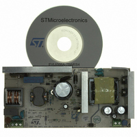
Manufacturer Part Number
EVL6566A-75WES4
Description
BOARD DEMO FOR L6563/LL6566A
Manufacturer
STMicroelectronics
Type
Power Factor Correctionr
Specifications of EVL6566A-75WES4
Main Purpose
AC/DC, Primary and Secondary Side with PFC
Outputs And Type
1, Isolated
Power - Output
75W
Voltage - Output
19V
Current - Output
4A
Voltage - Input
90 ~ 264VAC
Regulator Topology
Flyback
Board Type
Fully Populated
Utilized Ic / Part
L6563, L6566A, TSM1014
Input Voltage
90 V to 264 V
Output Voltage
19 V
Dimensions
78 mm x 170 mm
Product
Power Management Modules
Lead Free Status / RoHS Status
Lead free / RoHS Compliant
Frequency - Switching
-
Lead Free Status / Rohs Status
Lead free / RoHS Compliant
For Use With/related Products
L6563S, L6566A
Other names
497-8834
Available stocks
Company
Part Number
Manufacturer
Quantity
Price


List of figure
List of figure
Figure 1.
Figure 2.
Figure 3.
Figure 4.
Figure 5.
Figure 6.
Figure 7.
Figure 8.
Figure 9.
Figure 10.
Figure 11.
Figure 12.
Figure 13.
Figure 14.
Figure 15.
Figure 16.
Figure 17.
Figure 18.
Figure 19.
Figure 20.
Figure 21.
Figure 22.
Figure 23.
Figure 24.
Figure 25.
Figure 26.
Figure 27.
Figure 28.
Figure 29.
Figure 30.
Figure 31.
Figure 32.
Figure 33.
Figure 34.
Figure 35.
Figure 36.
Figure 37.
Figure 38.
Figure 39.
Figure 40.
Figure 41.
Figure 42.
Figure 43.
Figure 44.
Figure 45.
Figure 46.
Figure 47.
Figure 48.
4/43
Block diagram . . . . . . . . . . . . . . . . . . . . . . . . . . . . . . . . . . . . . . . . . . . . . . . . . . . . . . . . . . . . 1
Pin connection . . . . . . . . . . . . . . . . . . . . . . . . . . . . . . . . . . . . . . . . . . . . . . . . . . . . . . . . . . . 8
Typical system block diagram. . . . . . . . . . . . . . . . . . . . . . . . . . . . . . . . . . . . . . . . . . . . . . . 10
IC consumption vs VCC . . . . . . . . . . . . . . . . . . . . . . . . . . . . . . . . . . . . . . . . . . . . . . . . . . . 15
IC consumption vs TJ . . . . . . . . . . . . . . . . . . . . . . . . . . . . . . . . . . . . . . . . . . . . . . . . . . . . . 15
Vcc Zener voltage vs TJ . . . . . . . . . . . . . . . . . . . . . . . . . . . . . . . . . . . . . . . . . . . . . . . . . . . 15
Start-up and UVLO vs TJ . . . . . . . . . . . . . . . . . . . . . . . . . . . . . . . . . . . . . . . . . . . . . . . . . . 15
Feedback reference vs TJ . . . . . . . . . . . . . . . . . . . . . . . . . . . . . . . . . . . . . . . . . . . . . . . . . 16
E/A output clamp levels vs TJ. . . . . . . . . . . . . . . . . . . . . . . . . . . . . . . . . . . . . . . . . . . . . . . 16
UVLO saturation vs TJ . . . . . . . . . . . . . . . . . . . . . . . . . . . . . . . . . . . . . . . . . . . . . . . . . . . . 16
OVP levels vs TJ . . . . . . . . . . . . . . . . . . . . . . . . . . . . . . . . . . . . . . . . . . . . . . . . . . . . . . . . 16
Inductor saturation threshold vs TJ. . . . . . . . . . . . . . . . . . . . . . . . . . . . . . . . . . . . . . . . . . . 17
Vcs clamp vs TJ . . . . . . . . . . . . . . . . . . . . . . . . . . . . . . . . . . . . . . . . . . . . . . . . . . . . . . . . . 17
ZCD sink/source capability vs TJ . . . . . . . . . . . . . . . . . . . . . . . . . . . . . . . . . . . . . . . . . . . . 17
ZCD clamp level vs TJ . . . . . . . . . . . . . . . . . . . . . . . . . . . . . . . . . . . . . . . . . . . . . . . . . . . . 17
TBO clamp vs TJ . . . . . . . . . . . . . . . . . . . . . . . . . . . . . . . . . . . . . . . . . . . . . . . . . . . . . . . . 18
VVFF - VTBO dropout vs TJ . . . . . . . . . . . . . . . . . . . . . . . . . . . . . . . . . . . . . . . . . . . . . . . . 18
IINV - ITBO current mismatch vs TJ . . . . . . . . . . . . . . . . . . . . . . . . . . . . . . . . . . . . . . . . . . 18
IINV - ITBO mismatch vs ITBO current. . . . . . . . . . . . . . . . . . . . . . . . . . . . . . . . . . . . . . . . 18
R discharge vs TJ . . . . . . . . . . . . . . . . . . . . . . . . . . . . . . . . . . . . . . . . . . . . . . . . . . . . . . . . 19
Line drop detection threshold vs TJ . . . . . . . . . . . . . . . . . . . . . . . . . . . . . . . . . . . . . . . . . . 19
VMULTpk - VVFF dropout vs TJ. . . . . . . . . . . . . . . . . . . . . . . . . . . . . . . . . . . . . . . . . . . . . 19
PFC_OK threshold vs TJ . . . . . . . . . . . . . . . . . . . . . . . . . . . . . . . . . . . . . . . . . . . . . . . . . . 19
PFC_OK FFD threshold vs TJ . . . . . . . . . . . . . . . . . . . . . . . . . . . . . . . . . . . . . . . . . . . . . . 20
PWM_LATCH high saturation vs TJ . . . . . . . . . . . . . . . . . . . . . . . . . . . . . . . . . . . . . . . . . . 20
RUN threshold vs TJ. . . . . . . . . . . . . . . . . . . . . . . . . . . . . . . . . . . . . . . . . . . . . . . . . . . . . . 20
PWM_STOP low saturation vs TJ . . . . . . . . . . . . . . . . . . . . . . . . . . . . . . . . . . . . . . . . . . . 20
Multiplier characteristics @ VFF = 1 V . . . . . . . . . . . . . . . . . . . . . . . . . . . . . . . . . . . . . . . . 21
Multiplier characteristics @ VFF = 3 V . . . . . . . . . . . . . . . . . . . . . . . . . . . . . . . . . . . . . . . . 21
Multiplier gain vs TJ . . . . . . . . . . . . . . . . . . . . . . . . . . . . . . . . . . . . . . . . . . . . . . . . . . . . . . 21
Gate drive clamp vs TJ . . . . . . . . . . . . . . . . . . . . . . . . . . . . . . . . . . . . . . . . . . . . . . . . . . . . 21
Gate drive output saturation vs TJ . . . . . . . . . . . . . . . . . . . . . . . . . . . . . . . . . . . . . . . . . . . 22
Delay to output vs TJ . . . . . . . . . . . . . . . . . . . . . . . . . . . . . . . . . . . . . . . . . . . . . . . . . . . . . 22
Start-up timer period vs TJ . . . . . . . . . . . . . . . . . . . . . . . . . . . . . . . . . . . . . . . . . . . . . . . . . 22
Output voltage setting, OVP and FFP functions: internal block diagram . . . . . . . . . . . . . . 23
Voltage feedforward: squarer-divider (1/V2) block diagram and transfer characteristic . . 25
RFF·CFF as a function of 3rd harmonic distortion introduced in the input current . . . . . . . 26
THD optimizer circuit . . . . . . . . . . . . . . . . . . . . . . . . . . . . . . . . . . . . . . . . . . . . . . . . . . . . . 27
THD optimization: standard TM PFC controller (left side) and L6563S (right side) . . . . . . 28
Tracking boost block . . . . . . . . . . . . . . . . . . . . . . . . . . . . . . . . . . . . . . . . . . . . . . . . . . . . . . 30
Tracking output voltage vs Input voltage characteristic with TBO . . . . . . . . . . . . . . . . . . . 30
Effect of boost inductor saturation on the MOSFET current and detection method . . . . . . 31
Interface circuits that let dc-dc converter's controller IC drive L6563S in burst mode . . . . 32
Interface circuits that let the L6563S switch on or off a PWM controller. . . . . . . . . . . . . . . 32
Interface circuits for power up sequencing when dc-dc has the SS function . . . . . . . . . . . 33
Interface circuits for actual power-up sequencing (master PFC) . . . . . . . . . . . . . . . . . . . . 33
Brownout protection (master PFC) . . . . . . . . . . . . . . . . . . . . . . . . . . . . . . . . . . . . . . . . . . . 34
Demonstration board EVL6563S-100W, wide-range mains: electrical schematic . . . . . . . 35
Doc ID 16116 Rev 4
L6563S
Related parts for EVL6566A-75WES4
Image
Part Number
Description
Manufacturer
Datasheet
Request
R

Part Number:
Description:
BOARD EVAL FOR L6566A
Manufacturer:
STMicroelectronics
Datasheet:

Part Number:
Description:
STMicroelectronics [RIPPLE-CARRY BINARY COUNTER/DIVIDERS]
Manufacturer:
STMicroelectronics
Datasheet:
Part Number:
Description:
STMicroelectronics [LIQUID-CRYSTAL DISPLAY DRIVERS]
Manufacturer:
STMicroelectronics
Datasheet:

Part Number:
Description:
BOARD EVAL FOR MEMS SENSORS
Manufacturer:
STMicroelectronics
Datasheet:
Part Number:
Description:
NPN TRANSISTOR POWER MODULE
Manufacturer:
STMicroelectronics
Datasheet:
Part Number:
Description:
TURBOSWITCH ULTRA-FAST HIGH VOLTAGE DIODE
Manufacturer:
STMicroelectronics
Datasheet:
Part Number:
Description:
Manufacturer:
STMicroelectronics
Datasheet:
Part Number:
Description:
DIODE / SCR MODULE
Manufacturer:
STMicroelectronics
Datasheet:
Part Number:
Description:
DIODE / SCR MODULE
Manufacturer:
STMicroelectronics
Datasheet:
Part Number:
Description:
Search -----> STE16N100
Manufacturer:
STMicroelectronics
Datasheet:
Part Number:
Description:
Search ---> STE53NA50
Manufacturer:
STMicroelectronics
Datasheet:
Part Number:
Description:
NPN Transistor Power Module
Manufacturer:
STMicroelectronics
Datasheet: