NCP1230GEVB ON Semiconductor, NCP1230GEVB Datasheet - Page 5
NCP1230GEVB
Manufacturer Part Number
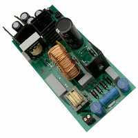
NCP1230GEVB
Description
EVAL BOARD FOR NCP1230G
Manufacturer
ON Semiconductor
Specifications of NCP1230GEVB
Design Resources
NCP1230 EVB BOM NCP1230GEVB Gerber Files NCP1230 EVB Schematic
Main Purpose
AC/DC, Primary Side
Outputs And Type
1, Isolated
Power - Output
90W
Voltage - Output
18.6V
Current - Output
4.74A
Voltage - Input
85 ~ 265VAC
Regulator Topology
Flyback
Frequency - Switching
47kHz
Board Type
Fully Populated
Utilized Ic / Part
NCP1230
Lead Free Status / RoHS Status
Lead free / RoHS Compliant
For Use With/related Products
NCP1230G
Other names
NCP1230GEVBOS


3. Verified by Design.
ELECTRICAL CHARACTERISTICS
V
Supply Section (All frequency versions, otherwise noted)
Internal Startup Current Source
Drive Output
Current Comparator and Thermal Shutdown
Turn−On Threshold Level, V
Minimum Operating Voltage after Turn−On
V
V
Internal IC Consumption, No Output Load on Pin 6 (V
Internal IC Consumption, 1.0 nF Output Load on Pin 6, F
Internal IC Consumption, 1.0 nF Output Load on Pin 6, F
Internal IC Consumption, 1.0 nF Output Load on Pin 6, F
Internal IC Consumption, Latch−Off Phase
High−Voltage Current Source, 1.0 nF Load
High−Voltage Current Source (V
Minimum Startup Voltage (I
Startup Leakage (V
Output Voltage Rise−Time @ C
Output Voltage Fall−Time @ C
Source Resistance, R
Sink Resistance, at 1.0 V on Pin 5 (V
Pin 1 Output Impedance (or R
Input Bias Current @ 1.0 V Input Level on Pin 3
Maximum Internal Current Setpoint
Default Internal Setpoint for Skip Cycle Operation and Standby
Default Internal Setpoint to Leave Standby
Propagation Delay from CS Detected to Gate Turned Off (V
Leading Edge Blanking Duration
Soft−Start Period (Note 3)
Temperature Shutdown, Maximum Value (Note 3)
Hysteresis while in Temperature Shutdown (Note 3)
CC
(V
(V
is closed) R
Detection
(Pin 5 Loaded by 1.0 nF)
CC
CC
fb
CCOFF
= 13 V, V
Decreasing Level at which the Latch−Off Phase Ends (V
Level at which the Internal Logic gets Reset
= 2.5 V)
−0.2 V, V
PIN8
load
on Pin 1 = 680 W
= 30 V unless otherwise noted.)
fb
PIN8
= 2.5 V, V
Load
= 500 V)
300 W (V
c
Characteristic
CC
= 0.5 mA, V
dson
L
PIN8
L
Going Up (V
= 1.0 nF, 10−90% of Output Signal
CC
= 1.0 nF, 10−90% of Output Signal
between Pin 1 and Pin 6 when SW1
= 0 V)
fb
= 30 V)
fb
= 2.5 V)
= 3.5 V)
CCOFF
(For typical values T
fb
= 2.0 V)
−0.2 V, V
Tj = −40°C to +125°C
fb
= 2.5 V)
SW
SW
SW
http://onsemi.com
fb
= 2.5 V)
Gate
= 65 kHz
= 100 kHz
= 133 kHz
J
fb
= 25°C, for min/max values T
Tj = 25°C
= 3.5 V)
= 10 V)
5
T
V
V
Symbol
V
V
T
V
V
I
SD
RPFC
HVLeak
CC(min)
stby−out
CClatch
CCreset
DEL CS
CCOFF
V
T
R
I
I
I
I
I
I
HVmin
R
T
CC1
CC2
CC2
CC2
CC3
Limit
SS
I
I
I
LEB
C1
C2
T
T
skip
OH
IB
SD
OL
hyste
r
f
J
Pin
= −40°C to +125°C, Max T
6
6
6
6
6
6
6
6
6
8
8
8
8
5
5
5
5
1
3
3
3
−
3
3
−
−
−
1.010
0.979
11.6
Min
400
600
100
150
7.0
5.0
0.6
1.3
1.3
1.3
1.8
1.8
6.0
3.0
6.0
1.0
10
−
−
−
−
−
−
−
−
1.063
12.6
12.3
0.02
1.25
11.7
Typ
680
750
200
165
7.7
5.6
4.0
1.1
1.8
2.2
2.8
3.2
4.4
7.5
2.5
20
30
40
15
90
25
−
J
1.127
1.116
1000
Max
13.6
= 150°C,
900
180
350
8.4
6.2
1.8
2.5
3.0
3.3
4.2
5.6
1.5
23
80
25
18
23
−
−
−
−
−
−
−
Unit
mA
mA
mA
mA
mA
mA
mV
ms
mA
mA
mA
ns
ns
ns
ns
°C
°C
W
W
W
V
V
V
V
V
V
V
Related parts for NCP1230GEVB
Image
Part Number
Description
Manufacturer
Datasheet
Request
R

Part Number:
Description:
Fixed Frequency Controller Featuring Pfc Go To Standby Function
Manufacturer:
ON Semiconductor
Datasheet:
Part Number:
Description:
ON Semiconductor [VOLTAGE REGULATOR]
Manufacturer:
ON Semiconductor
Datasheet:
Part Number:
Description:
357-036-542-201 CARDEDGE 36POS DL .156 BLK LOPRO
Manufacturer:
ON Semiconductor
Datasheet:
Part Number:
Description:
357-036-542-201 CARDEDGE 36POS DL .156 BLK LOPRO
Manufacturer:
ON Semiconductor
Datasheet:
Part Number:
Description:
357-036-542-201 CARDEDGE 36POS DL .156 BLK LOPRO
Manufacturer:
ON Semiconductor
Datasheet:
Part Number:
Description:
357-036-542-201 CARDEDGE 36POS DL .156 BLK LOPRO
Manufacturer:
ON Semiconductor
Datasheet:
Part Number:
Description:
357-036-542-201 CARDEDGE 36POS DL .156 BLK LOPRO
Manufacturer:
ON Semiconductor
Datasheet:
Part Number:
Description:
357-036-542-201 CARDEDGE 36POS DL .156 BLK LOPRO
Manufacturer:
ON Semiconductor
Datasheet:
Part Number:
Description:
357-036-542-201 CARDEDGE 36POS DL .156 BLK LOPRO
Manufacturer:
ON Semiconductor
Datasheet:
Part Number:
Description:
357-036-542-201 CARDEDGE 36POS DL .156 BLK LOPRO
Manufacturer:
ON Semiconductor
Datasheet:
Part Number:
Description:
357-036-542-201 CARDEDGE 36POS DL .156 BLK LOPRO
Manufacturer:
ON Semiconductor
Datasheet:
Part Number:
Description:
357-036-542-201 CARDEDGE 36POS DL .156 BLK LOPRO
Manufacturer:
ON Semiconductor
Datasheet:
Part Number:
Description:
Manufacturer:
ON Semiconductor
Datasheet:
Part Number:
Description:
Manufacturer:
ON Semiconductor
Datasheet: