NCP1230GEVB ON Semiconductor, NCP1230GEVB Datasheet - Page 2
NCP1230GEVB
Manufacturer Part Number
NCP1230GEVB
Description
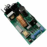
EVAL BOARD FOR NCP1230G
Manufacturer
ON Semiconductor
Specifications of NCP1230GEVB
Design Resources
NCP1230 EVB BOM NCP1230GEVB Gerber Files NCP1230 EVB Schematic
Main Purpose
AC/DC, Primary Side
Outputs And Type
1, Isolated
Power - Output
90W
Voltage - Output
18.6V
Current - Output
4.74A
Voltage - Input
85 ~ 265VAC
Regulator Topology
Flyback
Frequency - Switching
47kHz
Board Type
Fully Populated
Utilized Ic / Part
NCP1230
Lead Free Status / RoHS Status
Lead free / RoHS Compliant
For Use With/related Products
NCP1230G
Other names
NCP1230GEVBOS


PIN FUNCTION DESCRIPTION
HV
Pin No.
+
CBulk
1
2
3
4
5
6
7
8
MC33262/33260
1
2
3
4
Pin Name
PFC V
CS/OVP
GND
DRV
V
NC
HV
FB
CC
CC
8
7
6
5
This pin provides
the bias voltage to
the PFC controller.
Feedback Signal
Current Sense
IC Ground
Driver Output
V
High−Voltage
CC
Function
Input
−
PFC_V
Figure 1. Typical Application Example
OVP
CC
This pin is a direct connection to the V
standby and during the startup sequence, the switch is open and the PFC V
shut down. As soon as the aux. winding is stabilized, Pin 1 connects to the V
and provides bias to the PFC controller. It goes down in standby and fault conditions.
An optocoupler collector pulls this pin low to regulate. When the current setpoint
reaches 25% of the maximum peak, the controller skips cycles.
This pin incorporates three different functions: the current sense function, an internal
ramp compensation signal and a 3.0 V latch−off level which latches the output off
until V
With a drive capability of +500 mA / −800 mA, the NCP1230 can drive large Qg
MOSFETs.
The controller accepts voltages up to 18 V and features a UVLO turn−off threshold of
7.7 V typical.
This pin connects to the bulk voltage and offers a lossless startup sequence. The
charging current is high enough to support the bias needs of a PWM controller
through Pin 1.
http://onsemi.com
1
2
3
4
CC
Ramp Comp
NCP1230
is recycled.
10 k
2
8
7
6
5
OVP
Pin Description
V
CC
CC
Cap
pin (Pin 6) via a low impedance switch. In
−
−
Rsense
GN
D
+
CC
GND
CC
is
V
pin
out
Related parts for NCP1230GEVB
Image
Part Number
Description
Manufacturer
Datasheet
Request
R

Part Number:
Description:
Fixed Frequency Controller Featuring Pfc Go To Standby Function
Manufacturer:
ON Semiconductor
Datasheet:
Part Number:
Description:
ON Semiconductor [VOLTAGE REGULATOR]
Manufacturer:
ON Semiconductor
Datasheet:
Part Number:
Description:
357-036-542-201 CARDEDGE 36POS DL .156 BLK LOPRO
Manufacturer:
ON Semiconductor
Datasheet:
Part Number:
Description:
357-036-542-201 CARDEDGE 36POS DL .156 BLK LOPRO
Manufacturer:
ON Semiconductor
Datasheet:
Part Number:
Description:
357-036-542-201 CARDEDGE 36POS DL .156 BLK LOPRO
Manufacturer:
ON Semiconductor
Datasheet:
Part Number:
Description:
357-036-542-201 CARDEDGE 36POS DL .156 BLK LOPRO
Manufacturer:
ON Semiconductor
Datasheet:
Part Number:
Description:
357-036-542-201 CARDEDGE 36POS DL .156 BLK LOPRO
Manufacturer:
ON Semiconductor
Datasheet:
Part Number:
Description:
357-036-542-201 CARDEDGE 36POS DL .156 BLK LOPRO
Manufacturer:
ON Semiconductor
Datasheet:
Part Number:
Description:
357-036-542-201 CARDEDGE 36POS DL .156 BLK LOPRO
Manufacturer:
ON Semiconductor
Datasheet:
Part Number:
Description:
357-036-542-201 CARDEDGE 36POS DL .156 BLK LOPRO
Manufacturer:
ON Semiconductor
Datasheet:
Part Number:
Description:
357-036-542-201 CARDEDGE 36POS DL .156 BLK LOPRO
Manufacturer:
ON Semiconductor
Datasheet:
Part Number:
Description:
357-036-542-201 CARDEDGE 36POS DL .156 BLK LOPRO
Manufacturer:
ON Semiconductor
Datasheet:
Part Number:
Description:
Manufacturer:
ON Semiconductor
Datasheet:
Part Number:
Description:
Manufacturer:
ON Semiconductor
Datasheet: