NCP1230GEVB ON Semiconductor, NCP1230GEVB Datasheet - Page 7
NCP1230GEVB
Manufacturer Part Number
NCP1230GEVB
Description
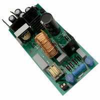
EVAL BOARD FOR NCP1230G
Manufacturer
ON Semiconductor
Specifications of NCP1230GEVB
Design Resources
NCP1230 EVB BOM NCP1230GEVB Gerber Files NCP1230 EVB Schematic
Main Purpose
AC/DC, Primary Side
Outputs And Type
1, Isolated
Power - Output
90W
Voltage - Output
18.6V
Current - Output
4.74A
Voltage - Input
85 ~ 265VAC
Regulator Topology
Flyback
Frequency - Switching
47kHz
Board Type
Fully Populated
Utilized Ic / Part
NCP1230
Lead Free Status / RoHS Status
Lead free / RoHS Compliant
For Use With/related Products
NCP1230G
Other names
NCP1230GEVBOS


Demo Board Test Procedure
the dc load to the J2 connector. Place a Digital Voltage Meter
(DVM) directly across the J2 output terminals. Set the ac
power source to 115 Vac, and turn on the ac source. The
NCP1230 controller will turn−on and supply 19 Vdc to the
+
Connect an ac power source to the J4 connector. Connect
−
ACMAG=1
NCP1230
averaged
Vin
200 Vdc
NCP1230 AV U7
IN
CoL
1 k
Vstim
C3
0.47 nF
LoL
1 k
FB
OUT
FS = 65 k
L = 0.22 mH
RI = 0.20
Figure 7. AC Frequency Response SPICE Model
U10
U9
R11
1 k
TL431
RATIO=0.1477
XFMR1
MOC8101
U6
R1
4.7 k
http://onsemi.com
AND8154/D
R7
0.16
7
C2
470 nF
load (refer to Table 1 for load regulation). Vary the load from
0 to 4.73 Adc and monitor the output voltage. Adjust the ac
power source from 85−265 Vac and monitor the output
voltage. Set the ac power source to 230 Vac, and disconnect
the dc load and monitor the standby power (refer to Table 4
for the standby power limits).
MUR810
D4
R2
49.9 k
R4
7.4 k
out1
C4
2200 mF
R3
0.022
C1
2200mF
R5
0.022
C5
2200mF
R8
0.022
C6
2200 mF
R6
0.022
2.2 mH
L1
Rload
C7
47 mF
3.9
Related parts for NCP1230GEVB
Image
Part Number
Description
Manufacturer
Datasheet
Request
R

Part Number:
Description:
Fixed Frequency Controller Featuring Pfc Go To Standby Function
Manufacturer:
ON Semiconductor
Datasheet:
Part Number:
Description:
ON Semiconductor [VOLTAGE REGULATOR]
Manufacturer:
ON Semiconductor
Datasheet:
Part Number:
Description:
357-036-542-201 CARDEDGE 36POS DL .156 BLK LOPRO
Manufacturer:
ON Semiconductor
Datasheet:
Part Number:
Description:
357-036-542-201 CARDEDGE 36POS DL .156 BLK LOPRO
Manufacturer:
ON Semiconductor
Datasheet:
Part Number:
Description:
357-036-542-201 CARDEDGE 36POS DL .156 BLK LOPRO
Manufacturer:
ON Semiconductor
Datasheet:
Part Number:
Description:
357-036-542-201 CARDEDGE 36POS DL .156 BLK LOPRO
Manufacturer:
ON Semiconductor
Datasheet:
Part Number:
Description:
357-036-542-201 CARDEDGE 36POS DL .156 BLK LOPRO
Manufacturer:
ON Semiconductor
Datasheet:
Part Number:
Description:
357-036-542-201 CARDEDGE 36POS DL .156 BLK LOPRO
Manufacturer:
ON Semiconductor
Datasheet:
Part Number:
Description:
357-036-542-201 CARDEDGE 36POS DL .156 BLK LOPRO
Manufacturer:
ON Semiconductor
Datasheet:
Part Number:
Description:
357-036-542-201 CARDEDGE 36POS DL .156 BLK LOPRO
Manufacturer:
ON Semiconductor
Datasheet:
Part Number:
Description:
357-036-542-201 CARDEDGE 36POS DL .156 BLK LOPRO
Manufacturer:
ON Semiconductor
Datasheet:
Part Number:
Description:
357-036-542-201 CARDEDGE 36POS DL .156 BLK LOPRO
Manufacturer:
ON Semiconductor
Datasheet:
Part Number:
Description:
Manufacturer:
ON Semiconductor
Datasheet:
Part Number:
Description:
Manufacturer:
ON Semiconductor
Datasheet: