NCP1230GEVB ON Semiconductor, NCP1230GEVB Datasheet - Page 6
NCP1230GEVB
Manufacturer Part Number
NCP1230GEVB
Description
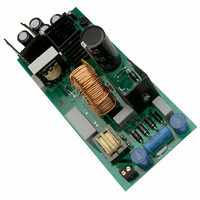
EVAL BOARD FOR NCP1230G
Manufacturer
ON Semiconductor
Specifications of NCP1230GEVB
Design Resources
NCP1230 EVB BOM NCP1230GEVB Gerber Files NCP1230 EVB Schematic
Main Purpose
AC/DC, Primary Side
Outputs And Type
1, Isolated
Power - Output
90W
Voltage - Output
18.6V
Current - Output
4.74A
Voltage - Input
85 ~ 265VAC
Regulator Topology
Flyback
Frequency - Switching
47kHz
Board Type
Fully Populated
Utilized Ic / Part
NCP1230
Lead Free Status / RoHS Status
Lead free / RoHS Compliant
For Use With/related Products
NCP1230G
Other names
NCP1230GEVBOS


regulation:
In this application R22 was changed to 1.0 kW to minimize
the stand by power consumption.
not be sufficient current through the optocoupler LED, so a
resistor (R7) is placed in parallel. A 4.7 kW resistor was
selected.
nominally 1.0, but over time the CTR will degrade so
analysis of the circuit with the CTR = 0.5 is recommended.
is a nominal 20 kW.
Standby Power
voltage sense resistor divider network was select to consume
less than 10 mW.
Control Loop
loop was stable, the results are shown below. The first
method was to use an Excel Spreadsheet (using the
previously derived equations) which can be down loaded
from the ON Semiconductor website (www://onsemi.com).
The results from the Excel Spreadsheet are shown below. At
full load and 200 Vdc (200 Vdc is the minimum voltage
being supplied from the PFC) the loop gain crosses zero dB
at approximately 1.2 kHz with approximately 100 of phase
margin.
Board in PSPICE. The result can be seen in Figure 6.
Because parasitic elements can be added to the PSPICE
model, it was more accurate at high frequencies.
shows similar results, the loop gain crosses zero dB at
approximately 1.2 kHz with about 90 of phase margin.
The TL431 requires a minimum of 1.0 mA of current for
When the power supply is operating at no load, there may
The optocoupler gain is:
CTR is the current transfer ratio of the opto and is
Rfb is the internal pull−up resistor of the NCP1230 and it
To minimize the standby power consumption, the output
The Standby power consumption is:
Standby power calculation:
Two methods were used to verify that the Demo Board
The second method was to model the NCP1230 Demo
The results from the PSPICE model (at low frequencies)
Vref + Vo
Ropto(R22) +
P_R22 + I 2 * R22 + 1 2 ma · 2 k + 2 mW
P_TL431 + (Vo * V_R22 * Vopto) · 1 ma
DVfb
DVc
P + Vo
dBgain + 20log20 + 26 dB
R10 ) R4
+ Rfb · CTR
+ 17 V · 1 ma + 17 mW
Rtotal
R10
Vo * Vfopto
Ropto
2
+ 19
1 mA
57400
+ 19
+ 20 · 1.0
2
+ 19 * 1
+ 6.3 mW
7.4 ) 50
1
1 mA
7.4
+ 20
+ 18 k
+ 2.5 V
http://onsemi.com
AND8154/D
6
−100
−100
−100
−140
−180
180
100
−20
−40
−60
−80
180
140
100
−20
−60
60
40
20
60
20
0
10 Hz
0
10
DB(V(FB))
10
Figure 5. Excel Spreadsheet Phase Margin
Figure 4. Excel Spreadsheet Loop Gain
100 Hz
P(V(FB))
100
100
Figure 6. SPICE Phase/Gain
Loop Gain Plot
Loop Phase Margin
FREQUENCY IN Hz
FREQUENCY
FREQUENCY
1.0 kHz
1000
1000
10000
10000
10 kHz
100000
100 kHz
100000
Related parts for NCP1230GEVB
Image
Part Number
Description
Manufacturer
Datasheet
Request
R

Part Number:
Description:
Fixed Frequency Controller Featuring Pfc Go To Standby Function
Manufacturer:
ON Semiconductor
Datasheet:
Part Number:
Description:
ON Semiconductor [VOLTAGE REGULATOR]
Manufacturer:
ON Semiconductor
Datasheet:
Part Number:
Description:
357-036-542-201 CARDEDGE 36POS DL .156 BLK LOPRO
Manufacturer:
ON Semiconductor
Datasheet:
Part Number:
Description:
357-036-542-201 CARDEDGE 36POS DL .156 BLK LOPRO
Manufacturer:
ON Semiconductor
Datasheet:
Part Number:
Description:
357-036-542-201 CARDEDGE 36POS DL .156 BLK LOPRO
Manufacturer:
ON Semiconductor
Datasheet:
Part Number:
Description:
357-036-542-201 CARDEDGE 36POS DL .156 BLK LOPRO
Manufacturer:
ON Semiconductor
Datasheet:
Part Number:
Description:
357-036-542-201 CARDEDGE 36POS DL .156 BLK LOPRO
Manufacturer:
ON Semiconductor
Datasheet:
Part Number:
Description:
357-036-542-201 CARDEDGE 36POS DL .156 BLK LOPRO
Manufacturer:
ON Semiconductor
Datasheet:
Part Number:
Description:
357-036-542-201 CARDEDGE 36POS DL .156 BLK LOPRO
Manufacturer:
ON Semiconductor
Datasheet:
Part Number:
Description:
357-036-542-201 CARDEDGE 36POS DL .156 BLK LOPRO
Manufacturer:
ON Semiconductor
Datasheet:
Part Number:
Description:
357-036-542-201 CARDEDGE 36POS DL .156 BLK LOPRO
Manufacturer:
ON Semiconductor
Datasheet:
Part Number:
Description:
357-036-542-201 CARDEDGE 36POS DL .156 BLK LOPRO
Manufacturer:
ON Semiconductor
Datasheet:
Part Number:
Description:
Manufacturer:
ON Semiconductor
Datasheet:
Part Number:
Description:
Manufacturer:
ON Semiconductor
Datasheet: