NCP5425SOEVB ON Semiconductor, NCP5425SOEVB Datasheet - Page 18
NCP5425SOEVB
Manufacturer Part Number
NCP5425SOEVB
Description
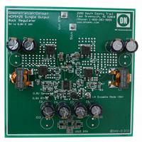
EVAL BOARD FOR NCP5425SO
Manufacturer
ON Semiconductor
Specifications of NCP5425SOEVB
Design Resources
NCP5425SOEVB BOM NCP5425SOEVB Gerber Files NCP5425SOEVB Schematic
Main Purpose
DC/DC, Step Down
Outputs And Type
1, Non-Isolated
Voltage - Output
0.8V
Current - Output
30A
Voltage - Input
4.6 ~ 12 V
Regulator Topology
Buck
Frequency - Switching
300kHz
Board Type
Fully Populated
Utilized Ic / Part
NCP5425
Lead Free Status / RoHS Status
Lead free / RoHS Compliant
Power - Output
-
Lead Free Status / Rohs Status
Lead free / RoHS Compliant
For Use With/related Products
NCP5425SO
Other names
NCP5425SOEVBOS


20 A. If an increased current limit is required, a resistor
divider can be added (see Figure 8). Advantages of setting
the current limit by using the winding resistance of the
inductor (relative to a sense resistor) are higher efficiency
and lower heat generation. The tolerance of the inductor
ESR must be factored into the design of the current limit.
Finally, one or two more components are required for this
approach than with resistor sensing.
Selecting and Configuring Current Sharing for a 2
Phase Single Output Application
two phase Buck Converter, they are in a Master−Slave
configuration. The Slave controller on the right side of
Figure 6 tries to follow information provided by the Master
controller, on the left. This circuit uses inductor current
sensing, in which the parasitic resistances (LSR) of the
controllers’ output chokes are used as current sensing
elements. On the Slave side (Controller Two), both Error
Amplifier inputs are brought to external pins so the
reference is available. The RC network in parallel with the
output inductor on the Master side (Controller One)
generates the reference for the Slave. Current information
from the Slave is fed back to the error amplifier’s inverting
input. In this configuration, the Slave tries to adjust its
current to match the current information fed to its reference
input from the Master Controller. If 50−50 current sharing
is needed, then Figure 8a is used for both sides to generate
the reference and the inverting signals. The values for both
sides should be calculated with the following equation:
constant, the voltage across the capacitor will be equal to the
voltage drop across the internal resistance of the inductor.
For proper sharing, the inductors on both Master and Slave
side should be the identical.
inductor sense resistor network selection is a three step
process:
resistors are designated R1, R2, and R3, as depicted in
Figures 12 and 13.
Given an ESR value of 3.5 mW, the current limit becomes
When the two controllers are connected as a single output
With the RC time constant selected to equal the L
If a current share ratio other than 50−50 is desired,
In the two examples that follow, the inductor sense
L
R
C1 = Select a value such that R1 is less than 15 KW.
x
x
1. Decide how the total load current will be budgeted
2. Calculate the value of R1 for the controller with
3. Calculate the current sense resistor network
= Inductor value, both controllers should use the same
= Internal resistance of L, from the inductor data sheet.
inductor.
between the two controllers.
the lesser current share.
(2 resistors) for the controller with the greater
current share.
R1 +
C1 · Rx
Lx
, where,
x
/R
http://onsemi.com
x
time
NCP5425
18
Example 1
current from the master controller, and 60% from the Slave.
Figure 12 shows the configuration of the inductor sense
networks and Slave error amplifier. The ratio of
Slave−to−Master load current is 60%/40%, or 1.5:1. R2 and
R3 must be chosen to satisfy two conditions:
Assume we have elected to source 40% of the output
A parallel equivalent resistance equal to R1, and,
A ratio such that the drop across the parasitic resistance of
the Slave inductor is 1.5 times the drop across the parasitic
resistance of the Master inductor when the inputs to the
Slave error amplifier are equal (assumes the inductors are
identical). The optimum value of R1 is described by the
equation:
Rx
Rx
Master
Switch
Master
Switch
Node
Node
Figure 13. 66.7%/33.3% Current Sharing
Figure 12. 40%/60% Current Sharing
Lx
Lx
R1
R2
R1 + Lx (C1 * Rx)
C1
C1
Output
DC
R3
Slave
Error
Amp
R3
Output
Slave
Error
Amp
DC
C1
C1
R2
R1
Lx
Lx
Switch
Switch
Slave
Slave
Node
Node
Rx
Rx
Related parts for NCP5425SOEVB
Image
Part Number
Description
Manufacturer
Datasheet
Request
R

Part Number:
Description:
Dual Synchronous Buck Controller
Manufacturer:
ON Semiconductor
Datasheet:
Part Number:
Description:
ON Semiconductor [VOLTAGE REGULATOR]
Manufacturer:
ON Semiconductor
Datasheet:
Part Number:
Description:
357-036-542-201 CARDEDGE 36POS DL .156 BLK LOPRO
Manufacturer:
ON Semiconductor
Datasheet:
Part Number:
Description:
357-036-542-201 CARDEDGE 36POS DL .156 BLK LOPRO
Manufacturer:
ON Semiconductor
Datasheet:
Part Number:
Description:
357-036-542-201 CARDEDGE 36POS DL .156 BLK LOPRO
Manufacturer:
ON Semiconductor
Datasheet:
Part Number:
Description:
357-036-542-201 CARDEDGE 36POS DL .156 BLK LOPRO
Manufacturer:
ON Semiconductor
Datasheet:
Part Number:
Description:
357-036-542-201 CARDEDGE 36POS DL .156 BLK LOPRO
Manufacturer:
ON Semiconductor
Datasheet:
Part Number:
Description:
357-036-542-201 CARDEDGE 36POS DL .156 BLK LOPRO
Manufacturer:
ON Semiconductor
Datasheet:
Part Number:
Description:
357-036-542-201 CARDEDGE 36POS DL .156 BLK LOPRO
Manufacturer:
ON Semiconductor
Datasheet:
Part Number:
Description:
357-036-542-201 CARDEDGE 36POS DL .156 BLK LOPRO
Manufacturer:
ON Semiconductor
Datasheet:
Part Number:
Description:
357-036-542-201 CARDEDGE 36POS DL .156 BLK LOPRO
Manufacturer:
ON Semiconductor
Datasheet:
Part Number:
Description:
357-036-542-201 CARDEDGE 36POS DL .156 BLK LOPRO
Manufacturer:
ON Semiconductor
Datasheet:
Part Number:
Description:
Manufacturer:
ON Semiconductor
Datasheet:
Part Number:
Description:
Manufacturer:
ON Semiconductor
Datasheet: