NCP5425SOEVB ON Semiconductor, NCP5425SOEVB Datasheet - Page 15
NCP5425SOEVB
Manufacturer Part Number
NCP5425SOEVB
Description
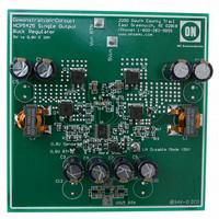
EVAL BOARD FOR NCP5425SO
Manufacturer
ON Semiconductor
Specifications of NCP5425SOEVB
Design Resources
NCP5425SOEVB BOM NCP5425SOEVB Gerber Files NCP5425SOEVB Schematic
Main Purpose
DC/DC, Step Down
Outputs And Type
1, Non-Isolated
Voltage - Output
0.8V
Current - Output
30A
Voltage - Input
4.6 ~ 12 V
Regulator Topology
Buck
Frequency - Switching
300kHz
Board Type
Fully Populated
Utilized Ic / Part
NCP5425
Lead Free Status / RoHS Status
Lead free / RoHS Compliant
Power - Output
-
Lead Free Status / Rohs Status
Lead free / RoHS Compliant
For Use With/related Products
NCP5425SO
Other names
NCP5425SOEVBOS


according to the formula:
where:
number of output capacitors can be calculated:
where:
be verified and compared to the value assigned by the
designer:
the following formula:
Input Inductor Selection
not disturb the input voltage. One method of achieving this
is by using an input inductor and a bypass capacitor. The
input inductor isolates the supply from the noise generated
in the switching portion of the buck regulator and also limits
the inrush current into the input capacitors during power up.
The inductor’s limiting effect on the input current slew rate
becomes increasingly beneficial during load transients. The
worst case is when the load changes from no load to full load
(load step), a condition under which the highest voltage
change across the input capacitors is also seen by the input
inductor. An input inductor successfully blocks the ripple
current while placing the transient current requirements on
the input bypass capacitor bank, which has to initially
support the sudden load change. The minimum value for the
input inductor is:
where:
that a minimum of 40 dB attenuation is obtained at the
regulator switching frequency. The LC filter is a
Maximum allowable ESR can then be determined
Once the maximum allowable ESR is determined, the
The actual output voltage deviation due to ESR can then
Similarly, the maximum allowable ESL is calculated from
A common requirement is that the buck controller must
The designer must select the LC filter pole frequency such
DV
ESR
ESR
L
DV = voltage seen by the input inductor during a full load
(dI/dt)
IN
ESR
= input inductor value;
CAP
MAX
swing;
MAX
=change in output voltage due to ESR
= maximum ESR per capacitor
(assigned by the designer)
Number of capacitors +
= maximum allowable ESR.
(specified in manufacturer’s data sheet);
DV ESR + DI OUT
= maximum allowable input current slew rate.
ESL MAX +
ESR MAX +
L IN +
(dl dt) MAX
DV ESL
DV
DV ESR
DI OUT
DI
ESR MAX
ESR CAP
ESR MAX
Dt
http://onsemi.com
NCP5425
15
double−pole network with a slope of −2.0, a roll−off rate of
−40 dB/decade, and a corner frequency given by:
where:
POWER FET SELECTION
FET Basics
two reasons: 1) high input impedance; and 2) fast switching
times. The electrical characteristics of a MOSFET are
considered to be nearly those of a perfect switch. Control
and drive circuitry power is therefore reduced. Because the
input impedance is so high, it is voltage driven. The input of
the MOSFET acts as if it were a small capacitor, which the
driving circuit must charge at turn on. The lower the drive
impedance, the higher the rate of rise of V
the turn−on time. Power dissipation in the switching
MOSFET consists of: (1) conduction losses, (2) leakage
losses, (3) turn−on switching losses, (4) turn−off switching
losses, and (5) gate−transitions losses. The latter three losses
are all proportional to frequency. The most important aspect
of FET performance is the Static Drain−to−Source
On−Resistance (R
efficiency and FET thermal management requirements. The
On−Resistance determines the amount of current a FET can
handle without excessive power dissipation that may cause
overheating and potentially catastrophic failure. As the
drain current rises, especially above the continuous rating,
the On−Resistance also increases. Its positive temperature
coefficient is between +0.6%/_C and +0.85%/_C. The
higher the On−Resistance, the larger the conduction loss is.
Additionally, the FET gate charge should be low in order to
minimize switching losses and reduce power dissipation.
Both logic level and standard FETs can be used. Voltage
applied to the FET gates depends on the application circuit
used. Both upper and lower gate driver outputs are specified
to drive to within 1.5 V of ground when in the low state and
to within 2.0 V of their respective bias supplies when in the
high state. In practice, the FET gates will be driven
rail−to−rail due to overshoot caused by the capacitive load
they present to the controller IC.
Switching (Upper) FET Selection
in the FET switch does not cause the power component’s
junction temperature to exceed 150_C. The maximum RMS
current through the switch can be determined by the
following formula:
I RMS(H) +
The use of a MOSFET as a power switch is compelled by
The designer must ensure that the total power dissipation
L = input inductor;
C = input capacitor(s).
I L(PEAK) 2 ) (I L(PEAK)
DS(ON)
f C +
),
2p
which
1
I L(VALLEY) ) ) I L(VALLEY) 2
LC
3
affects
GS
, and the faster
regulator
D
Related parts for NCP5425SOEVB
Image
Part Number
Description
Manufacturer
Datasheet
Request
R

Part Number:
Description:
Dual Synchronous Buck Controller
Manufacturer:
ON Semiconductor
Datasheet:
Part Number:
Description:
ON Semiconductor [VOLTAGE REGULATOR]
Manufacturer:
ON Semiconductor
Datasheet:
Part Number:
Description:
357-036-542-201 CARDEDGE 36POS DL .156 BLK LOPRO
Manufacturer:
ON Semiconductor
Datasheet:
Part Number:
Description:
357-036-542-201 CARDEDGE 36POS DL .156 BLK LOPRO
Manufacturer:
ON Semiconductor
Datasheet:
Part Number:
Description:
357-036-542-201 CARDEDGE 36POS DL .156 BLK LOPRO
Manufacturer:
ON Semiconductor
Datasheet:
Part Number:
Description:
357-036-542-201 CARDEDGE 36POS DL .156 BLK LOPRO
Manufacturer:
ON Semiconductor
Datasheet:
Part Number:
Description:
357-036-542-201 CARDEDGE 36POS DL .156 BLK LOPRO
Manufacturer:
ON Semiconductor
Datasheet:
Part Number:
Description:
357-036-542-201 CARDEDGE 36POS DL .156 BLK LOPRO
Manufacturer:
ON Semiconductor
Datasheet:
Part Number:
Description:
357-036-542-201 CARDEDGE 36POS DL .156 BLK LOPRO
Manufacturer:
ON Semiconductor
Datasheet:
Part Number:
Description:
357-036-542-201 CARDEDGE 36POS DL .156 BLK LOPRO
Manufacturer:
ON Semiconductor
Datasheet:
Part Number:
Description:
357-036-542-201 CARDEDGE 36POS DL .156 BLK LOPRO
Manufacturer:
ON Semiconductor
Datasheet:
Part Number:
Description:
357-036-542-201 CARDEDGE 36POS DL .156 BLK LOPRO
Manufacturer:
ON Semiconductor
Datasheet:
Part Number:
Description:
Manufacturer:
ON Semiconductor
Datasheet:
Part Number:
Description:
Manufacturer:
ON Semiconductor
Datasheet: