NCP1012GEVB ON Semiconductor, NCP1012GEVB Datasheet - Page 18
NCP1012GEVB
Manufacturer Part Number
NCP1012GEVB
Description
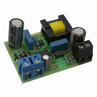
EVAL BOARD FOR NCP1012G
Manufacturer
ON Semiconductor
Specifications of NCP1012GEVB
Design Resources
NCP1012 Eval Brd BOM NCP1012GEVB Gerber Files NCP1012 Eval Brd Schematic
Main Purpose
AC/DC, Primary Side
Outputs And Type
1, Isolated
Voltage - Output
12V
Voltage - Input
230VAC
Regulator Topology
Flyback
Frequency - Switching
100kHz
Board Type
Fully Populated
Utilized Ic / Part
NCP1012
Lead Free Status / RoHS Status
Lead free / RoHS Compliant
Current - Output
-
Power - Output
-
Lead Free Status / Rohs Status
Lead free / RoHS Compliant
For Use With/related Products
NCP1012G
Other names
NCP1012GEVBOS


MOSFET Protection
drain excursion to a safe value, e.g. below the MOSFET
CVcc
Figure 27A: The simple capacitor limits the voltage
according to Equation 15. This option is only valid for low
power applications, e.g. below 5.0 W, otherwise chances
exist to destroy the MOSFET. After evaluating the leakage
inductance, you can compute C with Equation 15. Typical
values are between 100 pF and up to 470 pF. Large
capacitors increase capacitive losses.
Figure 27B: This diagram illustrates the most standard
circuitry called the RCD network. Rclamp and Cclamp are
calculated using the following formulas:
value N x (Vout + Vf). The diode needs to be a fast one and
a MUR160 represents a good choice. One major drawback
of the RCD network lies in its dependency upon the peak
current. Worse case occurs when Ip and Vin are maximum
and Vout is close to reach the steady- -state value.
Rclamp =
As in any Flyback design, it is important to limit the
Vclamp is usually selected 50- -80 V above the reflected
HV
+
+
Cclamp =
2 · Vclamp · (Vclamp − (Vout + Vf sec) · N)
1
2
3
4
NCP101X
A
Vripple · Fsw · Rclamp
Lleak · Ip 2 · Fsw
8
7
5
Vclamp
Figure 27. Different Options to Clamp the Leakage Spike
C
CVcc
HV
+
(eq. 27)
(eq. 28)
Rclamp
http://onsemi.com
1
2
3
4
18
NCP101X
B
BV
implementations:
Figure 27C: This option is probably the most expensive of
all three but it offers the best protection degree. If you need
a very precise clamping level, you must implement a Zener
diode or a TVS. There are little technology differences
behind a standard Zener diode and a TVS. However, the die
area is far bigger for a transient suppressor than that of Zener.
A 5.0 W Zener diode like the 1N5388B will accept 180 W
peak power if it lasts less than 8.3 ms. If the peak current in
the worse case (e.g. when the PWM circuit maximum
current limit works) multiplied by the nominal Zener
voltage exceeds these 180 W, then the diode will be
destroyed when the supply experiences overloads. A
transient suppressor like the P6KE200 still dissipates 5.0 W
of continuous power but is able to accept surges up to 600 W
@ 1.0 ms. Select the Zener or TVS clamping level between
40 to 80 V above the reflected output voltage when the
supply is heavily loaded.
DSS
Cclamp
8
7
5
D
which is 700 V. Figure 27 presents possible
CVcc
HV
+
1
2
3
4
Dz
NCP101X
C
8
7
5
D
Related parts for NCP1012GEVB
Image
Part Number
Description
Manufacturer
Datasheet
Request
R

Part Number:
Description:
Self−Supplied Monolithic Switcher for Low Standby−Power Offline SMPS
Manufacturer:
ONSEMI [ON Semiconductor]
Datasheet:

Part Number:
Description:
ON Semiconductor [VOLTAGE REGULATOR]
Manufacturer:
ON Semiconductor
Datasheet:
Part Number:
Description:
357-036-542-201 CARDEDGE 36POS DL .156 BLK LOPRO
Manufacturer:
ON Semiconductor
Datasheet:
Part Number:
Description:
357-036-542-201 CARDEDGE 36POS DL .156 BLK LOPRO
Manufacturer:
ON Semiconductor
Datasheet:
Part Number:
Description:
357-036-542-201 CARDEDGE 36POS DL .156 BLK LOPRO
Manufacturer:
ON Semiconductor
Datasheet:
Part Number:
Description:
357-036-542-201 CARDEDGE 36POS DL .156 BLK LOPRO
Manufacturer:
ON Semiconductor
Datasheet:
Part Number:
Description:
357-036-542-201 CARDEDGE 36POS DL .156 BLK LOPRO
Manufacturer:
ON Semiconductor
Datasheet:
Part Number:
Description:
357-036-542-201 CARDEDGE 36POS DL .156 BLK LOPRO
Manufacturer:
ON Semiconductor
Datasheet:
Part Number:
Description:
357-036-542-201 CARDEDGE 36POS DL .156 BLK LOPRO
Manufacturer:
ON Semiconductor
Datasheet:
Part Number:
Description:
357-036-542-201 CARDEDGE 36POS DL .156 BLK LOPRO
Manufacturer:
ON Semiconductor
Datasheet:
Part Number:
Description:
357-036-542-201 CARDEDGE 36POS DL .156 BLK LOPRO
Manufacturer:
ON Semiconductor
Datasheet:
Part Number:
Description:
357-036-542-201 CARDEDGE 36POS DL .156 BLK LOPRO
Manufacturer:
ON Semiconductor
Datasheet:
Part Number:
Description:
Manufacturer:
ON Semiconductor
Datasheet:
Part Number:
Description:
Manufacturer:
ON Semiconductor
Datasheet: