NCP1012GEVB ON Semiconductor, NCP1012GEVB Datasheet - Page 15
NCP1012GEVB
Manufacturer Part Number
NCP1012GEVB
Description
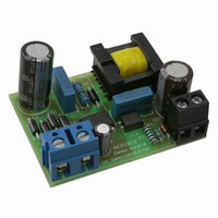
EVAL BOARD FOR NCP1012G
Manufacturer
ON Semiconductor
Specifications of NCP1012GEVB
Design Resources
NCP1012 Eval Brd BOM NCP1012GEVB Gerber Files NCP1012 Eval Brd Schematic
Main Purpose
AC/DC, Primary Side
Outputs And Type
1, Isolated
Voltage - Output
12V
Voltage - Input
230VAC
Regulator Topology
Flyback
Frequency - Switching
100kHz
Board Type
Fully Populated
Utilized Ic / Part
NCP1012
Lead Free Status / RoHS Status
Lead free / RoHS Compliant
Current - Output
-
Power - Output
-
Lead Free Status / Rohs Status
Lead free / RoHS Compliant
For Use With/related Products
NCP1012G
Other names
NCP1012GEVBOS


Full Latching Shutdown
when an abnormal situation is detected (overtemperature
or overvoltage). This feature can easily be implemented
through two external transistors wired as a discrete SCR.
When the OVP level exceeds the Zener breakdown
current flowing through Rhold should be small enough to let
the V
is fired. The NPN base can also receive a signal from a
temperature sensor. Typical bipolars can be MMBT2222
and MMBT2907 for the discrete latch. The MMBT3946
features two bipolars NPN+PNP in the same package and
could also be used.
Power Dissipation and Heatsinking
current- -source (when active) and the MOSFET. Thus,
Ptot = P
surrounded by copper, it becomes possible to drop its
thermal resistance junction- -to- -ambient, R
to 75C/W and thus dissipate more power. The
Other applications require a full latching shutdown, e.g.
Rhold ensures that the SCR stays on when fired. The bias
The NCP101X welcomes two dissipating terms, the DSS
CC
ramp up (8.5 V) and down (7.5 V) when the SCR
DSS
Figure 25. A Possible PCB Arrangement to Reduce the Thermal Resistance Junction- -to- -Ambient
+ P
Figure 24. Two Bipolars Ensure a Total Latch- -Off of the SMPS in Presence of an OVP
MOSFET
OVP
. When the PDIP- -7 package is
10 k
10 k
θJA
Rhold
BAT54
12 k
http://onsemi.com
down
15
voltage, the NPN biases the PNP and fires the equivalent
SCR, permanently bringing down the FB pin. The
switching pulses are disabled until the user unplugs the
power supply.
maximum power the device can thus evacuate is:
1.0 W for an ambient of 50C. The losses inherent to the
MOSFET R
formula:
is the worse case peak current (at the lowest line input), d is
the converter operating duty- -cycle and R
MOSFET resistance for T
valid for Discontinuous Conduction Mode (DCM)
operation where the turn- -on losses are null (the primary
current is zero when you restart the MOSFET). Figure 25
gives a possible layout to help drop the thermal resistance.
When measured on a 35 mm (1 oz) copper thickness PCB,
we obtained a thermal resistance of 75C/W.
Pmax =
+
CV
cc
1
2
3
4
T Jmax − Tambmax
Pmos = 1
DSon
R θJA
can be evaluated using the following
3
· Ip 2 · d · R DSon
8
7
5
J
= 100C. This formula is only
Drain
(eq. 12)
which gives around
(eq. 13)
DSon
, where Ip
, the
Related parts for NCP1012GEVB
Image
Part Number
Description
Manufacturer
Datasheet
Request
R

Part Number:
Description:
Self−Supplied Monolithic Switcher for Low Standby−Power Offline SMPS
Manufacturer:
ONSEMI [ON Semiconductor]
Datasheet:

Part Number:
Description:
ON Semiconductor [VOLTAGE REGULATOR]
Manufacturer:
ON Semiconductor
Datasheet:
Part Number:
Description:
357-036-542-201 CARDEDGE 36POS DL .156 BLK LOPRO
Manufacturer:
ON Semiconductor
Datasheet:
Part Number:
Description:
357-036-542-201 CARDEDGE 36POS DL .156 BLK LOPRO
Manufacturer:
ON Semiconductor
Datasheet:
Part Number:
Description:
357-036-542-201 CARDEDGE 36POS DL .156 BLK LOPRO
Manufacturer:
ON Semiconductor
Datasheet:
Part Number:
Description:
357-036-542-201 CARDEDGE 36POS DL .156 BLK LOPRO
Manufacturer:
ON Semiconductor
Datasheet:
Part Number:
Description:
357-036-542-201 CARDEDGE 36POS DL .156 BLK LOPRO
Manufacturer:
ON Semiconductor
Datasheet:
Part Number:
Description:
357-036-542-201 CARDEDGE 36POS DL .156 BLK LOPRO
Manufacturer:
ON Semiconductor
Datasheet:
Part Number:
Description:
357-036-542-201 CARDEDGE 36POS DL .156 BLK LOPRO
Manufacturer:
ON Semiconductor
Datasheet:
Part Number:
Description:
357-036-542-201 CARDEDGE 36POS DL .156 BLK LOPRO
Manufacturer:
ON Semiconductor
Datasheet:
Part Number:
Description:
357-036-542-201 CARDEDGE 36POS DL .156 BLK LOPRO
Manufacturer:
ON Semiconductor
Datasheet:
Part Number:
Description:
357-036-542-201 CARDEDGE 36POS DL .156 BLK LOPRO
Manufacturer:
ON Semiconductor
Datasheet:
Part Number:
Description:
Manufacturer:
ON Semiconductor
Datasheet:
Part Number:
Description:
Manufacturer:
ON Semiconductor
Datasheet: