STEVAL-ISA053V1 STMicroelectronics, STEVAL-ISA053V1 Datasheet - Page 24
STEVAL-ISA053V1
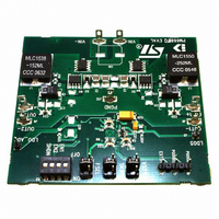
Manufacturer Part Number
STEVAL-ISA053V1
Description
BOARD EVALUATION FOR PM6680
Manufacturer
STMicroelectronics
Type
DC/DC Switching Converters, Regulators & Controllersr
Specifications of STEVAL-ISA053V1
Design Resources
STEVAL-ISA053V1 Gerber Files PM6680 Eval Kit Schematic STEVAL-ISA053V1 Bill of Material
Main Purpose
DC/DC, Step Down with LDO
Outputs And Type
3, Non-Isolated
Voltage - Output
1.05V, 1.5V, 5V
Current - Output
5A, 5A, 100mA
Voltage - Input
6 ~ 28V
Regulator Topology
Buck
Frequency - Switching
200kHz, 300kHz
Board Type
Fully Populated
Utilized Ic / Part
PM6680
Input Voltage
6 V to 28 V
Output Voltage
5 V
Product
Power Management Modules
Silicon Manufacturer
ST Micro
Silicon Core Number
PM6680
Kit Application Type
Power Management - Voltage Regulator
Application Sub Type
Step Down DC/DC Controller
Kit Contents
Board
Lead Free Status / RoHS Status
Lead free / RoHS Compliant
Power - Output
-
Lead Free Status / Rohs Status
Lead free / RoHS Compliant
For Use With/related Products
PM6680
Other names
497-6378
Available stocks
Company
Part Number
Manufacturer
Quantity
Price
Company:

Part Number:
STEVAL-ISA053V1
Manufacturer:
STMicroelectronics
Quantity:
1


Device description
7.3
24/49
Output ripple compensation and loop stability
In a classic Constant On Time control, the system regulates the valley value of the output
voltage and not the average value, as shown in
voltage ripple is source of a DC static error.
To compensate this error, an integrator network can be introduced in the control loop, by
connecting the output voltage to the COMP1/COMP2 (for the OUT1 and OUT2 sections
respectively) pin through a capacitor C
Figure 30. Circuitry for output ripple compensation
The integrator amplifier generates a current, proportional to the DC errors between the FB
voltage and Vr, which decreases the output voltage in order to compensate the total static
error, including the voltage drop on PCB traces. In addition, C
output ripple. In steady state, the voltage on COMP1/COMP2 pin is the sum of the reference
voltage Vr and the output ripple (see
reaches Vr, a fixed Ton begins and the output increases.
For example, we consider Vout = 5 V with an output ripple of ∆V = 50 mV. Considering
C
assures an AC path for the output voltage ripple. Then the COMP pin ripple is a replica of
the output ripple, with a DC value of Vr + 25 mV = 925 mV.
For more details about the output ripple compensation network, see the
Closing the integrator loop on page 37
In steady state the FB pin voltage is about Vr and the regulated output voltage depends on
the external divider:
Equation 4
INT
>> C
FILT
, the C
OUTPUT
VOLTAGE
Vr
INT
t
COMP PIN
VOLTAGE
DC voltage drop V
D
D
∆V
L
L
t
C
C
R
R
∆V
O
O
O
O
C
U
OUT
C
U
U
U
T
T
T
T
Figure
F
F
C
R
C
R
I
I
INT
L
L
in the Design guidelines.
I
I
I
I
T
T
N
N
N
N
T
T
T
T
=
CINT
as in
Vr
30). In fact when the voltage on the COMP pin
V
V
C
C
×
R
R
C
C
R
R
is about 5 V-Vr+25 mV = 4.125 V. C
O
Figure 30
O
I
I
Figure 28
N
N
⎛
⎝
2
2
1
1
O
O
T
T
1
M
M
U
U
+
F
F
P
P
T
T
B
B
R
------ -
R
2
1
I=gm(V1-Vr)
⎞
⎠
V
V
r
In this condition, the output
r
g
g
m
m
+
INT
V
V
1
1
V
V
provides an AC path for the
r
r
C
C
+
-
o
o
m
m
P
P
p
W
W
p
a
a
M
M
Section 7.13.6:
r
r
a
a
t
t
o
o
r
r
INT
PM6680
Related parts for STEVAL-ISA053V1
Image
Part Number
Description
Manufacturer
Datasheet
Request
R

Part Number:
Description:
BOARD RGB CTR ST7,STP08C596MTR
Manufacturer:
STMicroelectronics
Datasheet:

Part Number:
Description:
Power Management IC Development Tools Full Speed USB to RS232 Bridge Demo
Manufacturer:
STMicroelectronics
Datasheet:
Part Number:
Description:
Power Management IC Development Tools 2.5W solar eval BRD USB SPV1040 LD39050
Manufacturer:
STMicroelectronics
Datasheet:

Part Number:
Description:
BOARD EVAL FOR MEMS SENSORS
Manufacturer:
STMicroelectronics
Datasheet:

Part Number:
Description:
KIT DEV STARTER ST10F276Z5
Manufacturer:
STMicroelectronics
Datasheet:

Part Number:
Description:
BOARD EVAL HDMI $ VIDEO SWITCH
Manufacturer:
STMicroelectronics
Datasheet:

Part Number:
Description:
BOARD DEMO ACCELEROMETER DIL24
Manufacturer:
STMicroelectronics
Datasheet:

Part Number:
Description:
BOARD STLM75/STDS75/ST72F651
Manufacturer:
STMicroelectronics
Datasheet:

Part Number:
Description:
EVAL BOARD 3AXIS MEMS ACCELLRMTR
Manufacturer:
STMicroelectronics
Datasheet:

Part Number:
Description:
BOARD EVAL 8BIT MICRO + TDE1708
Manufacturer:
STMicroelectronics
Datasheet:
Part Number:
Description:
STMicroelectronics [RIPPLE-CARRY BINARY COUNTER/DIVIDERS]
Manufacturer:
STMicroelectronics
Datasheet:
Part Number:
Description:
STMicroelectronics [LIQUID-CRYSTAL DISPLAY DRIVERS]
Manufacturer:
STMicroelectronics
Datasheet:
Part Number:
Description:
BOARD EVAL FOR MEMS SENSORS
Manufacturer:
STMicroelectronics
Datasheet: