ADP2107-EVALZ Analog Devices Inc, ADP2107-EVALZ Datasheet - Page 6
ADP2107-EVALZ
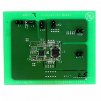
Manufacturer Part Number
ADP2107-EVALZ
Description
BOARD EVALUATION FOR ADP2107
Manufacturer
Analog Devices Inc
Specifications of ADP2107-EVALZ
Main Purpose
DC/DC, Step Down
Outputs And Type
1, Non-Isolated
Voltage - Output
2.5V
Current - Output
2A
Voltage - Input
2.7 ~ 5.5V
Regulator Topology
Buck
Frequency - Switching
1.2MHz
Board Type
Fully Populated
Utilized Ic / Part
ADP2107
Lead Free Status / RoHS Status
Lead free / RoHS Compliant
Power - Output
-


ADP2105/ADP2106/ADP2107
ABSOLUTE MAXIMUM RATINGS
Table 2.
Parameter
IN, EN, SS, COMP, FB to AGND
LX1, LX2 to PGND
PWIN1, PWIN2 to PGND
PGND to AGND
GND to AGND
PWIN1, PWIN2 to IN
Operating Junction Temperature Range
Storage Temperature Range
Soldering Conditions
Stresses above those listed under Absolute Maximum Ratings
may cause permanent damage to the device. This is a stress
rating only; functional operation of the device at these or any
other conditions above those indicated in the operational
section of this specification is not implied. Exposure to absolute
maximum rating conditions for extended periods may affect
device reliability.
Rating
−0.3 V to +6 V
−0.3 V to (V
−0.3 V to +6 V
−0.3 V to +0.3 V
−0.3 V to +0.3 V
−0.3 V to +0.3 V
−40°C to +125°C
−65°C to +150°C
JEDEC J-STD-020
IN
+ 0.3 V)
Rev. C | Page 6 of 36
THERMAL RESISTANCE
θ
soldered in a circuit board for surface-mount packages.
Table 3. Thermal Resistance
Package Type
16-Lead LFCSP_VQ/QFN
Maximum Power Dissipation
BOUNDARY CONDITION
Natural convection, 4-layer board, exposed pad soldered to the PCB.
ESD CAUTION
JA
is specified for the worst-case conditions, that is, a device
θ
40
1
JA
Unit
°C/W
W
Related parts for ADP2107-EVALZ
Image
Part Number
Description
Manufacturer
Datasheet
Request
R

Part Number:
Description:
BOARD EVAL FOR ADP2107-1.8
Manufacturer:
Analog Devices Inc
Datasheet:
Part Number:
Description:
Blank ADISimPower Eval ADP2107
Manufacturer:
Analog Devices Inc
Datasheet:
Part Number:
Description:
BOARD EVAL FOR ADP2107ACPZ-1.8
Manufacturer:
Analog Devices Inc
Datasheet:

Part Number:
Description:
±1.7g Dual-Axis IMEMS Accelerometer Evaluation Board
Manufacturer:
Analog Devices Inc
Datasheet:
Part Number:
Description:
Inertial Sensor Evaluation System
Manufacturer:
Analog Devices Inc
Datasheet:
Part Number:
Description:
Manufacturer:
Analog Devices Inc
Datasheet:
Part Number:
Description:
Manufacturer:
Analog Devices Inc
Datasheet:
Part Number:
Description:
Manufacturer:
Analog Devices Inc
Datasheet:
Part Number:
Description:
Manufacturer:
Analog Devices Inc
Datasheet:
Part Number:
Description:
Manufacturer:
Analog Devices Inc
Datasheet:
Part Number:
Description:
Manufacturer:
Analog Devices Inc
Datasheet:
Part Number:
Description:
Manufacturer:
Analog Devices Inc
Datasheet:
Part Number:
Description:
Manufacturer:
Analog Devices Inc
Datasheet: