ADP2107-EVALZ Analog Devices Inc, ADP2107-EVALZ Datasheet - Page 2
ADP2107-EVALZ
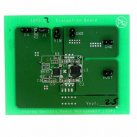
Manufacturer Part Number
ADP2107-EVALZ
Description
BOARD EVALUATION FOR ADP2107
Manufacturer
Analog Devices Inc
Specifications of ADP2107-EVALZ
Main Purpose
DC/DC, Step Down
Outputs And Type
1, Non-Isolated
Voltage - Output
2.5V
Current - Output
2A
Voltage - Input
2.7 ~ 5.5V
Regulator Topology
Buck
Frequency - Switching
1.2MHz
Board Type
Fully Populated
Utilized Ic / Part
ADP2107
Lead Free Status / RoHS Status
Lead free / RoHS Compliant
Power - Output
-


ADP2105/ADP2106/ADP2107
TABLE OF CONTENTS
Features .............................................................................................. 1
Applications ....................................................................................... 1
General Description ......................................................................... 1
Typical Operating Circuit ................................................................ 1
Revision History ............................................................................... 2
Functional Block Diagram .............................................................. 3
Specifications ..................................................................................... 4
Absolute Maximum Ratings ............................................................ 6
Pin Configuration and Function Descriptions ............................. 7
Typical Performance Characteristics ............................................. 8
Theory of Operation ...................................................................... 14
Applications Information .............................................................. 16
REVISION HISTORY
9/08—Rev. B to Rev. C
Changes to Table Summary Statement .......................................... 4
Changes to LX Minimum On-Time Parameter, Table 1 ............. 5
7/08—Rev. A to Rev. B
Changes to General Description Section ...................................... 1
Changes to Figure 3 .......................................................................... 3
Changes to Table 1 ............................................................................ 4
Changes to Table 2 ............................................................................ 6
Changes to Figure 4 .......................................................................... 7
Changes to Table 4 ............................................................................ 7
Changes to Figure 26 ...................................................................... 11
Changes to Figure 31 Through Figure 34 .................................... 12
Changes to Figure 35 ...................................................................... 13
Changes to PMW Mode Operation Section and Pulse Skipping
Threshold Section ........................................................................... 14
Changes to Slope Compensation Section .................................... 15
Changes to Setting the Output Voltage Section ........................ 16
Changes to Figure 37 ...................................................................... 16
Thermal Resistance ...................................................................... 6
Boundary Condition .................................................................... 6
ESD Caution .................................................................................. 6
Control Scheme .......................................................................... 14
PWM Mode Operation .............................................................. 14
PFM Mode Operation ................................................................ 14
Pulse-Skipping Threshold ......................................................... 14
100% Duty Cycle Operation (LDO Mode) ............................. 14
Slope Compensation .................................................................. 15
Design Features ........................................................................... 15
Rev. C | Page 2 of 36
Design Example .............................................................................. 24
External Component Recommendations .................................... 25
Circuit Board Layout Recommendations ................................... 27
Evaluation Board ............................................................................ 28
Application Circuits ....................................................................... 30
Outline Dimensions ....................................................................... 33
Changes to Inductor Selection Section ........................................ 17
Changes to Input Capacitor Selection Section ........................... 18
Changes to Figure 47 through Figure 52 ..................................... 21
Changes to Transition Losses Section and Thermal
Considerations Section .................................................................. 22
Changes to Table 11 ....................................................................... 25
Changes to Circuit Board Layout Recommendations Section..27
Changes to Table 12 ....................................................................... 26
Changes to Figure 53 ...................................................................... 28
Changes to Figure 56 Through Figure 57.................................... 30
Changes to Figure 58 Through Figure 59.................................... 31
Changes to Outline Dimensions .................................................. 33
3/07—Rev. 0 to Rev. A
Updated Format .................................................................. Universal
Changes to Output Characteristics and
LX (Switch Node) Characteristics Sections ................................... 3
Changes to Typical Performance Characteristics Section ........... 7
Changes to Load Transient Response Section ............................ 21
7/06—Revision 0: Initial Version
External Component Selection ................................................ 16
Setting the Output Voltage ........................................................ 16
Inductor Selection ...................................................................... 17
Output Capacitor Selection ....................................................... 18
Input Capacitor Selection .......................................................... 18
Input Filter ................................................................................... 19
Soft Start Period .......................................................................... 19
Loop Compensation .................................................................. 19
Bode Plots .................................................................................... 20
Load Transient Response .......................................................... 21
Efficiency Considerations ......................................................... 22
Thermal Considerations ............................................................ 22
Evaluation Board Schematic for ADP2107 (1.8 V) ............... 28
Recommended PCB Board Layout (Evaluation Board Layout)
....................................................................................................... 28
Ordering Guide .......................................................................... 33
Related parts for ADP2107-EVALZ
Image
Part Number
Description
Manufacturer
Datasheet
Request
R

Part Number:
Description:
BOARD EVAL FOR ADP2107-1.8
Manufacturer:
Analog Devices Inc
Datasheet:
Part Number:
Description:
Blank ADISimPower Eval ADP2107
Manufacturer:
Analog Devices Inc
Datasheet:
Part Number:
Description:
BOARD EVAL FOR ADP2107ACPZ-1.8
Manufacturer:
Analog Devices Inc
Datasheet:

Part Number:
Description:
±1.7g Dual-Axis IMEMS Accelerometer Evaluation Board
Manufacturer:
Analog Devices Inc
Datasheet:
Part Number:
Description:
Inertial Sensor Evaluation System
Manufacturer:
Analog Devices Inc
Datasheet:
Part Number:
Description:
Manufacturer:
Analog Devices Inc
Datasheet:
Part Number:
Description:
Manufacturer:
Analog Devices Inc
Datasheet:
Part Number:
Description:
Manufacturer:
Analog Devices Inc
Datasheet:
Part Number:
Description:
Manufacturer:
Analog Devices Inc
Datasheet:
Part Number:
Description:
Manufacturer:
Analog Devices Inc
Datasheet:
Part Number:
Description:
Manufacturer:
Analog Devices Inc
Datasheet:
Part Number:
Description:
Manufacturer:
Analog Devices Inc
Datasheet:
Part Number:
Description:
Manufacturer:
Analog Devices Inc
Datasheet: