ADP2107-EVALZ Analog Devices Inc, ADP2107-EVALZ Datasheet - Page 19
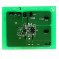
ADP2107-EVALZ
Manufacturer Part Number
ADP2107-EVALZ
Description
BOARD EVALUATION FOR ADP2107
Manufacturer
Analog Devices Inc
Specifications of ADP2107-EVALZ
Main Purpose
DC/DC, Step Down
Outputs And Type
1, Non-Isolated
Voltage - Output
2.5V
Current - Output
2A
Voltage - Input
2.7 ~ 5.5V
Regulator Topology
Buck
Frequency - Switching
1.2MHz
Board Type
Fully Populated
Utilized Ic / Part
ADP2107
Lead Free Status / RoHS Status
Lead free / RoHS Compliant
Power - Output
-


INPUT FILTER
The IN pin is the power source for the ADP2105/ADP2106/
ADP2107 internal circuitry, including the voltage reference and
current sense amplifier that are sensitive to power supply noise.
To prevent high frequency switching noise on the PWIN pins from
corrupting the internal circuitry of the ADP2105/ADP2106/
ADP2107, a low-pass RC filter should be placed between the IN
pin and the PWIN1 pin. The suggested input filter consists of
a small 0.1 μF ceramic capacitor placed between IN and AGND
and a 10 Ω resistor placed between IN and PWIN1. This forms a
150 kHz low-pass filter between PWIN1 and IN that prevents any
high frequency noise on PWIN1 from coupling into the IN pin.
SOFT START PERIOD
To set the soft start period, connect a soft start capacitor (C
SS to AGND. The soft start period varies linearly with the size
of the soft start capacitor, as shown in the following equation:
For a soft start period of 1 ms, a 1 nF capacitor must be
connected between SS and AGND.
LOOP COMPENSATION
The ADP2105/ADP2106/ADP2107 utilize a transconductance
error amplifier to compensate the external voltage loop. The
open loop transfer function at angular frequency (s) is given by
where:
V
V
Z
angular frequency.
C
g
nominal).
G
m
COMP
REF
OUT
OUT
CS
is the transconductance of the error amplifier (50 μA/V
is the effective transconductance of the current loop.
T
is the internal reference voltage (0.8 V).
G
G
G
is the output capacitor.
is the nominal output voltage.
H
(s) is the impedance of the compensation network at the
SS
CS
CS
CS
(
= C
s
= 1.875 A/V for the ADP2105.
= 2.8125 A/V for the ADP2106.
= 3.625 A/V for the ADP2107.
)
=
SS
G
× 10
m
G
CS
9
⎛
⎜
⎜
⎝
ms
Z
sC
COMP
OUT
(
s
)
⎞
⎟
⎟
⎠
⎛
⎜
⎜
⎝
V
V
OUT
REF
⎞
⎟
⎟
⎠
SS
) from
Rev. C | Page 19 of 36
The transconductance error amplifier drives the compensation
network that consists of a resistor (R
connected in series to form a pole and a zero, as shown in the
following equation:
At the crossover frequency, the gain of the open loop transfer
function is unity. For the compensation network impedance at
the crossover frequency, this yields the following equation:
where:
F
C
section.
To ensure that there is sufficient phase margin at the crossover
frequency, place the compensator zero at 1/4 of the crossover
frequency, as shown in the following equation:
Solving the three equations in this section simultaneously yields
the value for the compensation resistor and compensation
capacitor, as shown in the following equation:
CROSS
OUT
Z
V
C
Z
2 (
R
COMP
= 80 kHz, the crossover frequency of the loop.
OUT
COMP
COMP
COMP
) π
is determined from the Output Capacitor Selection
⎛
⎜
⎝
(
s
F
)
(
CROSS
=
F
=
=
4
CROSS
0
π
⎛
⎜
⎜
⎝
8 .
F
R
CROSS
COMP
⎞
⎟
⎠
⎛
⎜
⎜
⎝
ADP2105/ADP2106/ADP2107
)
R
2 (
=
COMP
2
G
) π
R
⎛
⎜
⎜
⎝
+
m
COMP
2 (
F
G
sC
C
CROSS
G
) π
CS
COMP
COMP
m
1
F
G
CROSS
CS
⎞
⎟
⎟
⎠
⎛
⎜
⎜
⎝
⎞
⎟
⎟
⎠
=
C
=
1
OUT
⎞
⎟
⎟
⎠
⎛ +
⎜
⎜
⎝
COMP
V
⎛
⎜
⎜
⎝
1
C
REF
V
OUT
) and capacitor (C
OUT
sR
V
sC
REF
COMP
V
COMP
OUT
⎞
⎟
⎟
⎠
C
COMP
⎞
⎟
⎟
⎠
⎞
⎟
⎟
⎠
COMP
)
Related parts for ADP2107-EVALZ
Image
Part Number
Description
Manufacturer
Datasheet
Request
R

Part Number:
Description:
BOARD EVAL FOR ADP2107-1.8
Manufacturer:
Analog Devices Inc
Datasheet:
Part Number:
Description:
Blank ADISimPower Eval ADP2107
Manufacturer:
Analog Devices Inc
Datasheet:
Part Number:
Description:
BOARD EVAL FOR ADP2107ACPZ-1.8
Manufacturer:
Analog Devices Inc
Datasheet:

Part Number:
Description:
±1.7g Dual-Axis IMEMS Accelerometer Evaluation Board
Manufacturer:
Analog Devices Inc
Datasheet:
Part Number:
Description:
Inertial Sensor Evaluation System
Manufacturer:
Analog Devices Inc
Datasheet:
Part Number:
Description:
Manufacturer:
Analog Devices Inc
Datasheet:
Part Number:
Description:
Manufacturer:
Analog Devices Inc
Datasheet:
Part Number:
Description:
Manufacturer:
Analog Devices Inc
Datasheet:
Part Number:
Description:
Manufacturer:
Analog Devices Inc
Datasheet:
Part Number:
Description:
Manufacturer:
Analog Devices Inc
Datasheet:
Part Number:
Description:
Manufacturer:
Analog Devices Inc
Datasheet:
Part Number:
Description:
Manufacturer:
Analog Devices Inc
Datasheet:
Part Number:
Description:
Manufacturer:
Analog Devices Inc
Datasheet: