CDB5532U Cirrus Logic Inc, CDB5532U Datasheet - Page 22
CDB5532U
Manufacturer Part Number
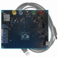
CDB5532U
Description
BOARD EVAL FOR CS5532U ADC
Manufacturer
Cirrus Logic Inc
Specifications of CDB5532U
Number Of Adc's
2
Number Of Bits
24
Sampling Rate (per Second)
3.84k
Data Interface
Serial
Inputs Per Adc
1 Differential
Input Range
±2.5 V
Power (typ) @ Conditions
35mW @ 3.84kSPS
Voltage Supply Source
Analog and Digital, Dual ±
Operating Temperature
-40°C ~ 85°C
Utilized Ic / Part
CS5532
Description/function
Audio DSPs
Operating Supply Voltage
5 V
Product
Audio Modules
For Use With/related Products
C8051F320
Lead Free Status / RoHS Status
Contains lead / RoHS non-compliant
Lead Free Status / RoHS Status
Lead free / RoHS Compliant, Contains lead / RoHS non-compliant
Other names
598-1159


2.2.4. Serial Port Interface
The CS5532/34’s serial interface consists of four
control lines: CS, SDI, SDO, SCLK. Figure 7 de-
tails the command and data word timing.
CS, Chip Select, is the control line which enables
access to the serial port. If the CS pin is tied low,
the port can function as a three wire interface.
SDI, Serial Data In, is the data signal used to trans-
fer data to the converters.
SDO, Serial Data Out, is the data signal used to
transfer output data from the converters. The SDO
output will be held at high impedance any time CS
is at logic 1.
22
SCLK
SCLK
SCLK
SDO
SDO
SDI
SDI
SDI
CS
CS
CS
* td is the time it takes the ADC to perform a conversion. See the Single
Conversion and Continuous Conversion sections of the data sheet for more
details about conversion timing.
Command Time
8 SCLKs
Command Time
Command Time
8 SCLKs
8 SCLKs
Figure 7. Command and Data Word Timing
t *
d
MSB
MSB
Data Conversion Cycle
8 SCLKs Clear SDO Flag
Write Cycle
Read Cycle
SCLK, Serial Clock, is the serial bit-clock which
controls the shifting of data to or from the ADC’s
serial port. The CS pin must be held low (logic 0)
before SCLK transitions can be recognized by the
port logic. To accommodate optoisolators SCLK is
designed with a Schmitt-trigger input to allow an
optoisolator with slower rise and fall times to di-
rectly drive the pin. Additionally, SDO is capable
of sinking or sourcing up to 5 mA to directly drive
an optoisolator LED. SDO will have less than a
400 mV loss in the drive voltage when sinking or
sourcing 5 mA.
Data Time 32 SCLKs
Data Time 32 SCLKs
MSB
Data Time 32 SCLKs
MCLK
Clock Cycles
CS5532/34-BS
/OWR
LSB
LSB
LSB
DS755F3
Related parts for CDB5532U
Image
Part Number
Description
Manufacturer
Datasheet
Request
R

Part Number:
Description:
Development Kit
Manufacturer:
Cirrus Logic Inc
Datasheet:
Part Number:
Description:
Development Kit
Manufacturer:
Cirrus Logic Inc
Datasheet:


Part Number:
Description:
High-efficiency PFC + Fluorescent Lamp Driver Reference Design
Manufacturer:
Cirrus Logic Inc
Datasheet:
Part Number:
Description:
Development Kit
Manufacturer:
Cirrus Logic Inc
Datasheet:
Part Number:
Description:
Development Kit
Manufacturer:
Cirrus Logic Inc
Datasheet:

Part Number:
Description:
Development Kit
Manufacturer:
Cirrus Logic Inc
Datasheet:
Part Number:
Description:
Development Kit
Manufacturer:
Cirrus Logic Inc
Datasheet:
Part Number:
Description:
Development Kit
Manufacturer:
Cirrus Logic Inc
Datasheet:
Part Number:
Description:
Development Kit
Manufacturer:
Cirrus Logic Inc
Datasheet:

Part Number:
Description:
EVALUATION BOARD FOR CS8427
Manufacturer:
Cirrus Logic Inc
Datasheet:

Part Number:
Description:
BOARD EVAL FOR CS8416 RCVR
Manufacturer:
Cirrus Logic Inc
Datasheet:

Part Number:
Description:
EVALUATION BOARD FOR CS8420
Manufacturer:
Cirrus Logic Inc
Datasheet:

Part Number:
Description:
KIT DEVELOPMENT EP9315 ARM9
Manufacturer:
Cirrus Logic Inc
Datasheet:

Part Number:
Description:
KIT DEVELOPMENT EP9302 ARM9
Manufacturer:
Cirrus Logic Inc
Datasheet: