EVAL-AD7731EBZ Analog Devices Inc, EVAL-AD7731EBZ Datasheet
EVAL-AD7731EBZ
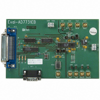
Manufacturer Part Number
EVAL-AD7731EBZ
Description
BOARD EVALUATION FOR AD7731
Manufacturer
Analog Devices Inc
Datasheets
1.AD7731BRUZ.pdf
(44 pages)
2.EVAL-AD7731EBZ.pdf
(11 pages)
3.EVAL-AD7731EBZ.pdf
(3 pages)
4.EVAL-AD7731EBZ.pdf
(44 pages)
Specifications of EVAL-AD7731EBZ
Number Of Adc's
1
Number Of Bits
24
Sampling Rate (per Second)
6.4k
Data Interface
Serial
Inputs Per Adc
3 Differential
Input Range
±1.28 V
Power (typ) @ Conditions
67.5mW @ 6.4kSPS
Voltage Supply Source
Analog and Digital
Operating Temperature
-40°C ~ 85°C
Utilized Ic / Part
AD7731
Lead Free Status / RoHS Status
Lead free / RoHS Compliant


ONE TECHNOLOGY WAY
INTRODUCTION
The AD7731 is a complete analog front-end for process
control applications. The device has a proprietary program-
mable gain front end which allows it to accept a range of
input signal ranges including low-level signals directly from
a transducer. The sigma delta architecture of the part
consists of an analog modulator and a low-pass program-
mable digital filter, allowing adjustment of filter cutoff,
output rate and settling-time.
The part features three buffered differential programmable
gain analog inputs (which can be configured as five pseudo-
differential inputs) as well as a differential reference input.
The part operates from a single +5 V supply and accepts
seven unipolar analog input ranges: 0 to +20 mV,
+40 mV, +80 mV, +160mV, +320 mV, +640 mV and
+1.28 V and seven bipolar ranges ±20 mV, ±40 mV,
±80 mV, ±160 mV, ±320 mV, ±640 mV and ±1.28 V.
The peak-to-peak resolution achievable directly from the
part is 16 bits at an 800 Hz output rate. The part can
switch between channels with 1ms settling time and
maintain a performance level of 13 bits of peak-to-peak
resolution.
The serial interface on the part can be configured for three-
wire operation and is compatible with microcontrollers and
digital signal processors. The AD7731 contains self-
calibration and system calibration options and features an
offset drift of less than 5nV/°C and a gain drift of less than
2ppm/°C.
As with all high resolution converters care has to be taken
with printed circuit board layout to achieve optimum
performance. The issues that give the greatest concern
include power supply decoupling, grounding techniques
and the general location of the digital and analog signals on
the printed circuit board. This technical note outlines
general guidlines on printed circuit board design and
layout in order to obtain the optimum performance from
the AD7731.
GROUNDING AND LAYOUT
Since the analog inputs and reference input are differential,
most of the voltages in the analog modulator are common-
mode voltages. The excellent Common-Mode Rejection of
the AD7731 will remove common-mode noise on these
inputs. The analog and digital supplies to the AD7731 are
independent and separately pinned out to minimize
coupling between the analog and digital sections of the
Obtaining Optimum Performance From the AD7731
•
P.O.BOX 9106
by: Albert O'Grady
•
NORWOOD, MASSACHUSETTS 02062-9106
Sigma Delta ADC
device. The digital filter will provide rejection of broad-
band noise on the power supplies, except at integer
multiples of the modulator sampling frequency. The digital
filter also removes noise from the analog and reference
inputs provided those noise sources do not saturate the
analog modulator. As a result, the AD7731 is more
immune to noise interference that a conventional high
resolution converter. However, because the resolution of
the AD7731 is so high and the noise levels from the
AD7731 so low, care must be taken with regard to ground-
ing and layout.
The printed circuit board which houses the AD7731 should
be designed such that the analog and digital sections are
separated and confined to certain areas of the board. This
facilitates the use of ground planes which can be separated
easily. A minimum etch technique is generally best for
ground planes as it gives the best shielding. Digital and
analog ground planes should only be joined in one place. If
the AD7731 is the only device requiring an AGND to
DGND connection, then the ground planes should be
connected at the AGND and DGND pins of the AD7731.
If the AD7731 is in a system where multiple devices require
AGND to DGND connections, the connection should still
be made at one point only, a star ground point which
should be established as close as possible to the AD7731.
Avoid running digital lines under the device as these will
couple noise onto the die. The analog ground plane should
be allowed to run under the AD7731 to avoid noise
coupling. The power supply lines to the AD7731 should
use as large a trace as possible to provide low impedance
paths and reduce the effects of glitches on the power supply
line. Fast switching signals like clocks should be shielded
with digital ground to avoid radiating noise to other
sections of the board and clock signals should never be run
near the analog inputs. Avoid crossover of digital and
analog signals. Traces on opposite sides of the board
should run at right angles to each other. This will reduce
the effects of feedthrough through the board. A microstrip
technique is by far the best but is not always possible with a
double-sided board. In this technique, the component side
of the board is dedicated to ground planes while signals are
placed on the solder side.
Good decoupling is important when using high resolution
ADCs. All analog supplies should be decoupled with 10µF
tantalum in parallel with 0.1µF capacitors to AGND. To
Technical Note
•
781/329-4700
Related parts for EVAL-AD7731EBZ
Image
Part Number
Description
Manufacturer
Datasheet
Request
R


Part Number:
Description:
BOARD EVAL FOR SI270X-A
Manufacturer:
Silicon Laboratories Inc
Datasheet:

Part Number:
Description:
BUCK CONV REF DESIGN KIT IP1201
Manufacturer:
International Rectifier
Datasheet:
Part Number:
Description:
BOARD DEMO SYNC DUAL BUCK CNVTER
Manufacturer:
International Rectifier
Datasheet:
Part Number:
Description:
BOARD DEMO SYNC BUCK CONVETER
Manufacturer:
International Rectifier
Datasheet:

Part Number:
Description:
EVALBOARD/EB Omnidirectional microphone - Analog
Manufacturer:
Analog Devices
Datasheet:
Part Number:
Description:
EVALBOARD/EB Omnidirectional microphone - Analog
Manufacturer:
Analog Devices
Datasheet:


Part Number:
Description:
BOARD EVAL LED DRIVER LT3756
Manufacturer:
Linear Technology
Datasheet:

Part Number:
Description:
BOARD EVAL FOR AD7741/7742
Manufacturer:
Analog Devices Inc
Datasheet:

Part Number:
Description:
±1.7g Dual-Axis IMEMS Accelerometer Evaluation Board
Manufacturer:
Analog Devices Inc
Datasheet:

Part Number:
Description:
IC MULTIPLIER ANALOG 8-SOIC T/R
Manufacturer:
Analog Devices Inc
Datasheet:

Part Number:
Description:
IC ANALOG MULTIPLIER 8-DIP
Manufacturer:
Analog Devices Inc
Datasheet:
Part Number:
Description:
IC ANALOG MULTIPLIER 8-SOIC
Manufacturer:
Analog Devices Inc
Datasheet:
Part Number:
Description:
IC ANALOG MULTIPLIER 8-DIP
Manufacturer:
Analog Devices Inc
Datasheet:
EVAL-AD7731EBZ Summary of contents
Page 1
ONE TECHNOLOGY WAY P.O.BOX 9106 Obtaining Optimum Performance From the AD7731 INTRODUCTION The AD7731 is a complete analog front-end for process control applications. The device has a proprietary program- mable gain front end which allows it to accept a ...
Page 2
... A full evaluation board package including a fully as- sembled and tested evaluation board, documentation, software for controlling the board over the printer port and software for analyzing the AD7731’s performance on the PC is available from Analog Devices. The evaluation board order number is EVAL-AD7731EB ...
Page 3
... Figure 2. Eval-AD7731EB Solder Side Artwork. Figure 3. Eval-AD7731EB Silkscreen Artwork ...