EVAL-AD7684CBZ Analog Devices Inc, EVAL-AD7684CBZ Datasheet - Page 13
EVAL-AD7684CBZ
Manufacturer Part Number
EVAL-AD7684CBZ
Description
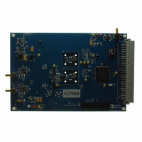
BOARD EVALUATION FOR AD7684
Manufacturer
Analog Devices Inc
Series
PulSAR®r
Specifications of EVAL-AD7684CBZ
Number Of Adc's
1
Number Of Bits
16
Sampling Rate (per Second)
100k
Data Interface
Serial
Inputs Per Adc
2 Single
Input Range
±VREF
Power (typ) @ Conditions
4mW @ 5 V, 100kSPS
Voltage Supply Source
Single Supply
Operating Temperature
-40°C ~ 85°C
Utilized Ic / Part
AD7684
Lead Free Status / RoHS Status
Lead free / RoHS Compliant


TYPICAL CONNECTION DIAGRAM
Figure 22 shows an example of the recommended application
diagram for the AD7684.
ANALOG INPUTS
The analog inputs (+IN, −IN) need to be driven differentially
180° from each other, as shown in Figure 22. Holding either
input at GND or a fixed dc gives erroneous conversion results
because the AD7684 is intended for differential operation only.
For applications requiring –IN to be at GND (±100 mV), the
AD7683
Figure 23 shows an equivalent circuit of the input structure of
the AD7684. The two diodes, D1 and D2, provide ESD protection
for the analog inputs, +IN and −IN. Care must be taken to
ensure that the analog input signal never exceeds the supply
rails by more than 0.3 V because this causes these diodes to
become forward-biased and start conducting current. However,
these diodes can handle a forward-biased current of 130 mA
maximum. For instance, these conditions could eventually
occur when the supplies of the input buffer (U1) are different
from VDD. In such a case, an input buffer with a short-circuit
current limitation can be used to protect the part.
This analog input structure allows the sampling of the differential
signal between +IN and −IN. By using this differential input, small
signals common to both inputs are rejected. During the acquisition
phase, the impedance of the analog inputs can be modeled as a
parallel combination of the Capacitor C
formed by the series connection of R
OR –IN
GND
+IN
should be used.
Figure 23. Equivalent Analog Input Circuit
C
PIN
VDD
0 TO V
V
NOTE 1: SEE VOLTAGE REFERENCE INPUT SECTION FOR REFERENCE SELECTION.
NOTE 2: C
NOTE 3: SEE DRIVER AMPLIFIER CHOICE SECTION.
NOTE 4: OPTIONAL FILTER. SEE ANALOG INPUT SECTION.
NOTE 5: SEE DIGITAL INTERFACE FOR MOST CONVENIENT INTERFACE MODE.
REF
D1
D2
TO 0
REF
(NOTE 3)
(NOTE 3)
REF
IS USUALLY A 10μF CERAMIC CAPACITOR (X5R).
IN
and C
PIN
R
IN
and the network
IN
(NOTE 4)
(NOTE 4)
2.7nF
2.7nF
33Ω
33Ω
. C
C
PIN
IN
(NOTE 1)
REF
is primarily
Figure 22. Typical Application Diagram
2.2μF TO 10μF
(NOTE 2)
Rev. A | Page 13 of 16
+IN
–IN
REF
GND
AD7684
the pin capacitance. R
component made up of some serial resistors and the on-
resistance of the switches. C
the ADC sampling capacitor. During the conversion phase,
when the switches are opened, the input impedance is limited
to C
undesirable aliasing effects and limits the noise.
When the source impedance of the driving circuit is low, the
AD7684 can be driven directly. Large source impedances
significantly affect the ac performance, especially THD. The dc
performances are less sensitive to the input impedance.
DRIVER AMPLIFIER CHOICE
Although the AD7684 is easy to drive, the driver amplifier
needs to meet the following requirements:
•
•
•
PIN
The noise generated by the driver amplifier needs to be
kept as low as possible to preserve the SNR and transition
noise performance of the AD7684. Note that the AD7684
has a noise level much lower than most other 16-bit ADCs
and, therefore, can be driven by a noisier op amp while
preserving the same or better system performance. The
noise coming from the driver is filtered by the AD7684
analog input circuit 1-pole, low-pass filter made by R
C
For ac applications, the driver needs to have a THD
performance commensurate with the AD7684. Figure 15
shows the THD vs. frequency that the driver should exceed.
For multichannel multiplexed applications, the driver
amplifier and the AD7684 analog input circuit must be
able to settle for a full-scale step of the capacitor array at a
16-bit level (0.0015%). In the data sheet of the amplifier,
settling at 0.1% to 0.01% is more commonly specified. This
could differ significantly from the settling time at a 16-bit
level and should be verified prior to driver selection.
IN
. R
VDD
DCLOCK
or by the external filter, if one is used.
IN
D
and C
OUT
CS
100nF
IN
make a 1-pole, low-pass filter that reduces
IN
is typically 600 Ω and is a lumped
3-WIRE INTERFACE
2.7V TO 5.25V
IN
is typically 30 pF and is mainly
AD7684
IN
and
Related parts for EVAL-AD7684CBZ
Image
Part Number
Description
Manufacturer
Datasheet
Request
R


Part Number:
Description:
BOARD EVAL FOR SI270X-A
Manufacturer:
Silicon Laboratories Inc
Datasheet:

Part Number:
Description:
BUCK CONV REF DESIGN KIT IP1201
Manufacturer:
International Rectifier
Datasheet:
Part Number:
Description:
BOARD DEMO SYNC DUAL BUCK CNVTER
Manufacturer:
International Rectifier
Datasheet:
Part Number:
Description:
BOARD DEMO SYNC BUCK CONVETER
Manufacturer:
International Rectifier
Datasheet:

Part Number:
Description:
EVALBOARD/EB Omnidirectional microphone - Analog
Manufacturer:
Analog Devices
Datasheet:
Part Number:
Description:
EVALBOARD/EB Omnidirectional microphone - Analog
Manufacturer:
Analog Devices
Datasheet:


Part Number:
Description:
BOARD EVAL LED DRIVER LT3756
Manufacturer:
Linear Technology
Datasheet:

Part Number:
Description:
BOARD EVAL FOR AD7741/7742
Manufacturer:
Analog Devices Inc
Datasheet:

Part Number:
Description:
±1.7g Dual-Axis IMEMS Accelerometer Evaluation Board
Manufacturer:
Analog Devices Inc
Datasheet:

Part Number:
Description:
IC MULTIPLIER ANALOG 8-SOIC T/R
Manufacturer:
Analog Devices Inc
Datasheet:

Part Number:
Description:
IC ANALOG MULTIPLIER 8-DIP
Manufacturer:
Analog Devices Inc
Datasheet:
Part Number:
Description:
IC ANALOG MULTIPLIER 8-SOIC
Manufacturer:
Analog Devices Inc
Datasheet:
Part Number:
Description:
IC ANALOG MULTIPLIER 8-DIP
Manufacturer:
Analog Devices Inc
Datasheet: