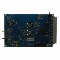
EVAL-AD7684CBZ Analog Devices Inc, EVAL-AD7684CBZ Datasheet

EVAL-AD7684CBZ
Specifications of EVAL-AD7684CBZ
Related parts for EVAL-AD7684CBZ
EVAL-AD7684CBZ Summary of contents
Page 1
FEATURES 16-bit resolution with no missing codes Throughput: 100 kSPS INL: ±1 LSB typical, ±3 LSB maximum True differential analog input range: ± with VDD on both inputs REF REF Single-supply operation: 2.7 ...
Page 2
... Changes to Table 6 and Layout ....................................................... 6 Changes to Table 7............................................................................ 7 Changes to Figure 15 Caption....................................................... 10 Changes to Figure 21...................................................................... 12 Changes to Figure 22 and Analog Inputs Section ...................... 13 Changes to Table 9, Digital Interface Section, and Evaluating the Performance of the AD7684 Section..................................... 14 Updated Outline Dimensions ....................................................... 15 Changes to Ordering Guide .......................................................... 15 Converter Operation.................................................................. 12 Transfer Functions ..................................................................... 12 Typical Connection Diagram ...
Page 3
SPECIFICATIONS VDD = 2 5 VDD; T REF A Table 2. Parameter Conditions RESOLUTION ANALOG INPUT 1 Voltage Range +IN − (−IN) Absolute Input Voltage +IN, −IN Common-Mode Input Range +IN, −IN Analog Input CMRR ...
Page 4
AD7684 VDD = VDD −40°C to +85°C, unless otherwise noted. REF A Table 3. Parameter Conditions ACCURACY No Missing Codes Integral Linearity Error Transition Noise 1 Gain Error MIN MAX Gain ...
Page 5
TIMING SPECIFICATIONS VDD = 2 5 −40°C to +85°C, unless otherwise noted. A Table 5. Parameter Throughput Rate CS Falling to DCLOCK Low CS Falling to DCLOCK Rising DCLOCK Falling to Data Remains Valid CS ...
Page 6
AD7684 ABSOLUTE MAXIMUM RATINGS Table 6. Parameter Rating Analog Inputs 1 1 +IN , −IN GND − 0 VDD + 0 ±130 mA REF GND − 0 VDD + 0.3 V Supply Voltages VDD ...
Page 7
PIN CONFIGURATION AND FUNCTION DESCRIPTIONS Table 7. Pin Function Descriptions 1 Pin No. Mnemonic Type Description 1 REF AI Reference Input Voltage. The REF range is from 0 VDD. This pin is referred to the GND pin and ...
Page 8
AD7684 TERMINOLOGY Integral Nonlinearity Error (INL) Linearity error refers to the deviation of each individual code from a line drawn from negative full scale through positive full scale. The point used as negative full scale occurs ½ LSB before the ...
Page 9
TYPICAL PERFORMANCE CHARACTERISTICS 3 POSITIVE INL = +0.83LSB NEGATIVE INL = –1.07LSB –1 –2 –3 0 16384 32768 CODE Figure 7. Integral Nonlinearity vs. Code 120000 94794 100000 80000 60000 40000 18557 17388 20000 0 0 151 ...
Page 10
AD7684 100 95 S/[N+D] 90 ENOB 85 80 2.0 2.5 3.0 3.5 4.0 REFERENCE VOLTAGE (V) Figure 13. SNR, SINAD, and ENOB vs. Reference Voltage 100 VREF = 5V, –10dB 95 VREF = 5V, –1dB 90 VREF = 2.5V, –1dB ...
Page 11
ZERO ERROR 1 0 –1 –2 GAIN ERROR –3 –4 –5 –6 –55 –35 – TEMPERATURE (°C) Figure 19. Zero Error and Gain Error vs. Temperature 85 105 125 Rev. A ...
Page 12
AD7684 APPLICATION INFORMATION +IN REF GND –IN CIRCUIT INFORMATION The AD7684 is a low power, single-supply, 16-bit ADC using a successive approximation architecture capable of converting 100,000 samples per second (100 kSPS) and powers down between conversions. When ...
Page 13
TO V REF (NOTE REF (NOTE 3) NOTE 1: SEE VOLTAGE REFERENCE INPUT SECTION FOR REFERENCE SELECTION. NOTE USUALLY A 10μF CERAMIC CAPACITOR (X5R). REF NOTE 3: SEE DRIVER AMPLIFIER CHOICE SECTION. ...
Page 14
... EVALUATING THE PERFORMANCE OF THE AD7684 Other recommended layouts for the AD7684 are outlined in the evaluation board for the AD7684 (EVAL-AD7684CBZ). The 10k 100k evaluation board package includes a fully assembled and tested ...
Page 15
... LSB maximum AD7684BRMZ 1 ±3 LSB maximum 1 AD7684BRMZRL7 ±3 LSB maximum 1, 2 EVAL-AD7684CBZ 1, 3 EVAL-CONTROL BRD3Z RoHS Compliant Part. 2 This board can be used as a standalone evaluation board or in conjunction with the EVAL-CONTROL BRDx for evaluation/demonstration purposes. 3 This board allows control and communicate with all the Analog Devices, Inc. evaluation boards ending in the CB designators. ...
Page 16
AD7684 NOTES ©2004–2007 Analog Devices, Inc. All rights reserved. Trademarks and registered trademarks are the property of their respective owners. D04302-0-10/07(A) Rev Page ...


