EVAL-AD7678CB Analog Devices Inc, EVAL-AD7678CB Datasheet
EVAL-AD7678CB
Specifications of EVAL-AD7678CB


Related parts for EVAL-AD7678CB


EVAL-AD7678CB Summary of contents
Page 1
FEATURES 18-bit resolution with no missing codes No pipeline delay (SAR architecture) Differential input range: ± REF REF Throughput: 100 kSPS INL: ±2.5 LSB max (±9.5 ppm of full scale) Dynamic range: 103 dB typ ...
Page 2
... Removed Endnote 3 from DC Accuracy; Zero Error Parameter; Table 2 ................................................................... 3 MAX Changes to Endnote 3, Table 2 ........................................................ 4 Moved ESD Caution ......................................................................... 7 Changes to Figure 4 and Table 6 ..................................................... 8 Changes to Evaluating the AD7678’s Performance Section ...... 25 Updated Outline Dimensions ....................................................... 26 Changes to Ordering Guide .......................................................... 26 8/03—Revision 0: Initial Version Digital Interface .......................................................................... 20 ...
Page 3
SPECIFICATIONS Table 2. –40°C to +85° 4.096 V, AVDD = DVDD = 5 V, OVDD = 2 5.25 V, unless otherwise noted. REF Parameter RESOLUTION ANALOG INPUT Voltage Range Operating Input Voltage Analog Input CMRR Input ...
Page 4
AD7678 Parameter DIGITAL INPUTS Logic Levels DIGITAL OUTPUTS 5 Data Format Pipeline Delay POWER SUPPLIES Specified Performance AVDD DVDD OVDD Operating Current AVDD 8 DVDD 8 OVDD ...
Page 5
TIMING SPECIFICATIONS Table 3. –40°C to +85°C, AVDD = DVDD = 5 V, OVDD = 2 5.25 V, unless otherwise noted. Parameter Refer to Figure 27 and Figure 28 Convert Pulse Width Time between Conversions CNVST LOW to ...
Page 6
AD7678 Table 4. Serial Clock Timings in Master Read after Convert DIVSCLK[1] DIVSCLK[0] SYNC to SCLK First Edge Delay Minimum Internal SCLK Period Minimum Internal SCLK Period Maximum Internal SCLK HIGH Minimum Internal SCLK LOW Minimum SDOUT Valid Setup Time ...
Page 7
ABSOLUTE MAXIMUM RATINGS Table 5. AD7678 Absolute Maximum Ratings Parameter Analog Inputs 2 2 IN+ , IN– , REF, REFBUFIN, REFGND to AGND Ground Voltage Differences AGND, DGND, OGND Supply Voltages AVDD, DVDD, OVDD AVDD to DVDD, AVDD to OVDD ...
Page 8
AD7678 PIN CONFIGURATION AND FUNCTION DESCRIPTIONS Figure 4. 48-Lead LQFP and 48-Lead LFCSP (ST-48 and CP-48) Pin Configuration Table 6. Pin Function Descriptions 1 Pin No. Mnemonic Type Description 1, 44 AGND P Analog Power Ground Pin AVDD ...
Page 9
Pin No. Mnemonic Type Description 13 D6 DI/O In all modes except MODE = 3, this output is used as Bit 6 of the parallel port data output bus. or EXT/INT When MODE = 3 (serial mode), this input, ...
Page 10
AD7678 1 Pin No. Mnemonic Type Description Power-Down Input. When set to a logic HIGH, power consumption is reduced and conversions are inhibited after the current one is completed. 35 CNVST DI Start Conversion. If CNVST is ...
Page 11
DEFINITION OF SPECIFICATIONS Integral Nonlinearity Error (INL) Linearity error refers to the deviation of each individual code from a line drawn from negative full scale through positive full scale. The point used as negative full scale occurs ½ LSB before ...
Page 12
AD7678 TYPICAL PERFORMANCE CHARACTERISTICS 2.5 2.0 1.5 1.0 0.5 0 –0.5 –1.0 –1.5 –2.0 –2.5 0 65536 131072 CODE Figure 5. Integral Nonlinearity vs. Code 70000 60158 59966 60000 50000 40000 30000 20000 10000 5919 20015 ...
Page 13
THD –120 THIRD HARMONIC HARMONIC –130 –140 –150 FREQUENCY (kHz) Figure 11. THD and Harmonics vs. Frequency 104 V 103 102 101 100 99 98 –60 –50 –40 –30 –20 INPUT LEVEL ...
Page 14
AD7678 GAIN ERROR ZERO ERROR –10 –20 –30 –40 –50 –55 –35 – TEMPERATURE ( C) Figure 17. Zero Error and Gain Error vs. Temperature 65 85 105 125 03083-0-022 ...
Page 15
CIRCUIT INFORMATION IN+ REF REFGND IN– The AD7678 is a very fast, low power, single-supply, precise 18-bit analog-to-digital converter (ADC) using successive approximation architecture. The AD7678’s linearity and dynamic range are similar or better than many - ADCs. With the ...
Page 16
AD7678 Transfer Functions Except in 18-bit interface mode, the AD7678 offers straight binary and twos complement output coding when using OB See Figure 20 and Table 8 for the ideal transfer characteristic. 111...111 111...110 111...101 000...010 000...001 000...000 ...
Page 17
TYPICAL CONNECTION DIAGRAM Figure 21 shows a typical connection diagram for the AD7678. Different circuitry shown on this diagram is optional and is discussed later in this data sheet. Analog Inputs Figure 22 shows a simplified analog input section of ...
Page 18
AD7678 The AD8021 meets these requirements and is usually appropri- ate for almost all applications. The AD8021 needs external compensation capacitor, which should have good linearity as an NPO ceramic or mica type. The AD8022 could be ...
Page 19
POWER DISSIPATION VERSUS THROUGHPUT The AD7678 automatically reduces its power consumption at the end of each conversion phase. During the acquisition phase, the operating currents are very low, which allows for a signifi- cant power savings when the conversion rate ...
Page 20
AD7678 DIGITAL INTERFACE The AD7678 has a versatile digital interface; it can be interfaced with the host system by using either a serial or parallel interface. The serial interface is multiplexed on the parallel data bus. The AD7678 digital interface ...
Page 21
MASTER SERIAL INTERFACE Internal Clock The AD7678 is configured to generate and provide the serial data clock SCLK when the EXT/ INT pin is held low. The AD7678 also generates a SYNC signal to indicate to the host when the ...
Page 22
AD7678 EXT/INT = 0 CS, RD CNVST BUSY t 17 SYNC SCLK t X SDOUT Figure 34. Master Serial Data Timing for Reading (Read Previous Conversion during Convert) SLAVE SERIAL INTERFACE External ...
Page 23
EXT/INT = 1 CS BUSY SCLK SDOUT X D17 D16 SDIN X17 X16 t 33 Figure 35. Slave Serial Data Timing for Reading ...
Page 24
AD7678 BUSY AD7678 #2 (UPSTREAM) #1 (DOWNSTREAM) RDC/SDIN SDOUT RDC/SDIN CNVST CS SCLK SCLK CNVST IN Figure 37. Two AD7678s in a Daisy-Chain Configuration External Clock Data Read during Conversion Figure 36 shows the detailed timing diagrams ...
Page 25
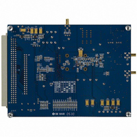
... The evaluation board for the AD7678 allows a quick means to measure both dc (histograms and time domain) and ac (time and frequency domain) performances of the converter. The EVAL-AD7678CBZ is an evaluation board package that includes a fully assembled and tested evaluation board, documentation, and software. The accompanying software requires the use of a capture board that must be ordered seperately from the evalua- tion board (see the Ordering Guide for information) ...
Page 26
... AD7678ASTZRL –40°C to +85°C 1 AD7678ACPZ –40°C to +85°C 1 AD7678ACPZRL –40°C to +85°C 2 EVAL-AD7678CBZ 1, 3 EVAL-CONTROL BRD2Z 1, 3 EVAL-CONTROL BRD3Z 1, 3 EVAL-CED1Z RoHS Compliant Part. 2 This board can be used as a standalone evaluation board or in conjunction with the a capture board for evaluation/demonstration purposes. ...
Page 27
NOTES Rev Page AD7678 ...
Page 28
AD7678 NOTES ©2003–2009 Analog Devices, Inc. All rights reserved. Trademarks and registered trademarks are the property of their respective companies. D03084-0-6/09(A) Rev Page ...