CDB5560 Cirrus Logic Inc, CDB5560 Datasheet - Page 28
CDB5560
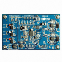
Manufacturer Part Number
CDB5560
Description
DEV BOARD FOR CS5560 W/MUX
Manufacturer
Cirrus Logic Inc
Type
A/Dr
Specifications of CDB5560
Number Of Adc's
1
Number Of Bits
24
Sampling Rate (per Second)
50k
Data Interface
Serial
Inputs Per Adc
1 Differential
Input Range
±3 V
Power (typ) @ Conditions
90mW @ 2.5 V
Voltage Supply Source
Dual ±
Operating Temperature
-40°C ~ 85°C
Utilized Ic / Part
CS5560
Product
Data Conversion Development Tools
Conversion Rate
50 KSPS
Resolution
24 bit
Maximum Clock Frequency
16 MHz
Interface Type
SPI
Supply Voltage (max)
3.3 V
Supply Voltage (min)
- 2.5 V
For Use With/related Products
CS5560
Lead Free Status / RoHS Status
Contains lead / RoHS non-compliant
Lead Free Status / RoHS Status
Lead free / RoHS Compliant, Contains lead / RoHS non-compliant
Other names
598-1273
CDB5560-1
CDB5560-1


4. PIN DESCRIPTIONS
28
VREF+, VREF- – Voltage Reference Input, Pins 9, 10
AIN+, AIN- – Differential Analog Input, Pins 4, 5
SMODE – Serial Mode Select, Pin 3
BUFEN – Buffer Enable, Pin 8
TST – Factory Test, Pin 2
V1+ – Positive Power 1, Pin 7
V1- – Negative Power 1, Pin 6
CS – Chip Select, Pin 1
Voltage Reference Input
Voltage Reference Input
Differential Analog Input
Differential Analog Input
Bipolar/Unipolar Select
The Chip Select pin allows an external device to access the serial port. If SMODE = VL (SSC
Mode) and CS is held high, the SDO output and the SCLK output will be held in a
high-impedance output state.
For factory use only. Connect to VLR.
The serial interface mode pin (SMODE) dictates whether the serial port behaves as a master or
slave interface. If SMODE is tied high (to VL), the port will operate in the Synchronous
Self-Clocking (SSC) mode. In SSC mode, the port acts as a master in which the converter out-
puts both the SDO and SCLK signals. If SMODE is tied low (to VLR), the port will operate in the
Synchronous External Clocking (SEC) mode. In SEC mode, the port acts as a slave in which
the external logic or microcontroller generates the SCLK used to output the conversion data
word from the SDO pin.
AIN+ and AIN- are differential inputs for the converter.
The V1- and V2- pins provide a negative supply voltage to the core circuitry of the chip. These
two pins should be decoupled as shown in the application block diagrams. V1- and V2- should
be supplied from the same source voltage. For single-supply operation, these two voltages are
nominally 0 V (Ground). For dual-supply operation, they are nominally -2.5 V.
The V1+ and V2+ pins provide a positive supply voltage to the core circuitry of the chip. These
two pins should be decoupled as shown in the application block diagrams. V1+ and V2+ should
be supplied from the same source voltage. For single-supply operation, these two voltages are
nominally +5 V. For dual-supply operation, they are nominally +2.5 V.
Buffers on input pins AIN+ and AIN- are enabled if BUFEN is connected to V1+ and disabled if
connected to V1-.
A differential voltage reference input on these pins functions as the voltage reference for the
converter. The voltage between these pins can range between 2.4 volts and 4.2 volts, with
4.096 volts being the nominal reference voltage value.
Serial Mode Select
Sleep Mode Select
Negative Power 1
Positive Power 1
Buffer Enable
Factory Test
Chip Select
SMODE
BUFEN
SLEEP
VREF+
BP/UP
VREF-
AIN+
AIN-
TST
V1+
V1-
CS
1
2
3
4
5
6
7
8
9
10
11
12
5/4/09
24
23
22
21
20
19
18
17
16
15
14
13
RDY
SCLK
SDO
VL
VLR
MCLK
V2-
V2+
DCR
CONV
VLR2
RST
Ready
Serial Clock Input/Output
Serial Data Output
Logic Interface Power
Logic Interface Return
Master Clock
Negative Voltage 2
Positive Voltage 2
Digital Core Regulator
Convert
Logic Interface Return
Reset
CS5560
DS713PP2
Related parts for CDB5560
Image
Part Number
Description
Manufacturer
Datasheet
Request
R

Part Number:
Description:
Development Kit
Manufacturer:
Cirrus Logic Inc
Datasheet:
Part Number:
Description:
Development Kit
Manufacturer:
Cirrus Logic Inc
Datasheet:


Part Number:
Description:
High-efficiency PFC + Fluorescent Lamp Driver Reference Design
Manufacturer:
Cirrus Logic Inc
Datasheet:
Part Number:
Description:
Development Kit
Manufacturer:
Cirrus Logic Inc
Datasheet:
Part Number:
Description:
Development Kit
Manufacturer:
Cirrus Logic Inc
Datasheet:

Part Number:
Description:
Development Kit
Manufacturer:
Cirrus Logic Inc
Datasheet:
Part Number:
Description:
Development Kit
Manufacturer:
Cirrus Logic Inc
Datasheet:
Part Number:
Description:
Development Kit
Manufacturer:
Cirrus Logic Inc
Datasheet:
Part Number:
Description:
Development Kit
Manufacturer:
Cirrus Logic Inc
Datasheet:

Part Number:
Description:
EVALUATION BOARD FOR CS8427
Manufacturer:
Cirrus Logic Inc
Datasheet:

Part Number:
Description:
BOARD EVAL FOR CS8416 RCVR
Manufacturer:
Cirrus Logic Inc
Datasheet:

Part Number:
Description:
EVALUATION BOARD FOR CS8420
Manufacturer:
Cirrus Logic Inc
Datasheet:

Part Number:
Description:
KIT DEVELOPMENT EP9315 ARM9
Manufacturer:
Cirrus Logic Inc
Datasheet:

Part Number:
Description:
KIT DEVELOPMENT EP9302 ARM9
Manufacturer:
Cirrus Logic Inc
Datasheet: