CDB5560 Cirrus Logic Inc, CDB5560 Datasheet - Page 14
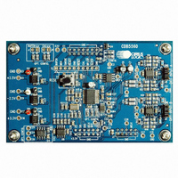
CDB5560
Manufacturer Part Number
CDB5560
Description
DEV BOARD FOR CS5560 W/MUX
Manufacturer
Cirrus Logic Inc
Type
A/Dr
Specifications of CDB5560
Number Of Adc's
1
Number Of Bits
24
Sampling Rate (per Second)
50k
Data Interface
Serial
Inputs Per Adc
1 Differential
Input Range
±3 V
Power (typ) @ Conditions
90mW @ 2.5 V
Voltage Supply Source
Dual ±
Operating Temperature
-40°C ~ 85°C
Utilized Ic / Part
CS5560
Product
Data Conversion Development Tools
Conversion Rate
50 KSPS
Resolution
24 bit
Maximum Clock Frequency
16 MHz
Interface Type
SPI
Supply Voltage (max)
3.3 V
Supply Voltage (min)
- 2.5 V
For Use With/related Products
CS5560
Lead Free Status / RoHS Status
Contains lead / RoHS non-compliant
Lead Free Status / RoHS Status
Lead free / RoHS Compliant, Contains lead / RoHS non-compliant
Other names
598-1273
CDB5560-1
CDB5560-1


5/4/09
CS5560
To perform only one conversion, CONV should return high at least 20 master clock cycles before RDY
falls.
Once a conversion is completed and RDY falls, RDY will return high when all the bits of the data word are
emptied from the serial port or if the conversion data is not read and CS is held low, RDY will go high two
MCLK cycles before the end of conversion. RDY will fall at the end of the next conversion when new data
is put into the port register.
See
Serial Port
on page 24 for information about reading conversion data.
Conversion performance can be affected by several factors. These include the choice of clock source for
the chip, the timing of CONV, and the choice of the serial port mode.
The converter can be operated from an internal oscillator. This clock source has greater jitter than an ex-
ternal crystal-based clock. Jitter may not be an issue when measuring DC signals, or very-low-frequency
AC signals, but can become an issue for higher frequency AC signals. For maximum performance when
digitizing AC signals, a low-jitter MCLK should be used.
To maximize performance, the CONV pin should be held low in the continuous conversion state to per-
form multiple conversions, or CONV should occur synchronous to MCLK, falling when MCLK falls.
If the converter is operated at maximum throughput, the SSC serial port mode is less likely to cause in-
terference to measurements as the SCLK output is synchronized to the MCLK. Alternately, any interfer-
ence due to serial port clocking can also be minimized if data is read in the SEC serial port mode when a
conversion is not in progress.
14
DS713PP2
Related parts for CDB5560
Image
Part Number
Description
Manufacturer
Datasheet
Request
R

Part Number:
Description:
Development Kit
Manufacturer:
Cirrus Logic Inc
Datasheet:
Part Number:
Description:
Development Kit
Manufacturer:
Cirrus Logic Inc
Datasheet:


Part Number:
Description:
High-efficiency PFC + Fluorescent Lamp Driver Reference Design
Manufacturer:
Cirrus Logic Inc
Datasheet:
Part Number:
Description:
Development Kit
Manufacturer:
Cirrus Logic Inc
Datasheet:
Part Number:
Description:
Development Kit
Manufacturer:
Cirrus Logic Inc
Datasheet:

Part Number:
Description:
Development Kit
Manufacturer:
Cirrus Logic Inc
Datasheet:
Part Number:
Description:
Development Kit
Manufacturer:
Cirrus Logic Inc
Datasheet:
Part Number:
Description:
Development Kit
Manufacturer:
Cirrus Logic Inc
Datasheet:
Part Number:
Description:
Development Kit
Manufacturer:
Cirrus Logic Inc
Datasheet:

Part Number:
Description:
EVALUATION BOARD FOR CS8427
Manufacturer:
Cirrus Logic Inc
Datasheet:

Part Number:
Description:
BOARD EVAL FOR CS8416 RCVR
Manufacturer:
Cirrus Logic Inc
Datasheet:

Part Number:
Description:
EVALUATION BOARD FOR CS8420
Manufacturer:
Cirrus Logic Inc
Datasheet:

Part Number:
Description:
KIT DEVELOPMENT EP9315 ARM9
Manufacturer:
Cirrus Logic Inc
Datasheet:

Part Number:
Description:
KIT DEVELOPMENT EP9302 ARM9
Manufacturer:
Cirrus Logic Inc
Datasheet: