CDB5560 Cirrus Logic Inc, CDB5560 Datasheet - Page 9
CDB5560
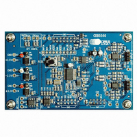
Manufacturer Part Number
CDB5560
Description
DEV BOARD FOR CS5560 W/MUX
Manufacturer
Cirrus Logic Inc
Type
A/Dr
Specifications of CDB5560
Number Of Adc's
1
Number Of Bits
24
Sampling Rate (per Second)
50k
Data Interface
Serial
Inputs Per Adc
1 Differential
Input Range
±3 V
Power (typ) @ Conditions
90mW @ 2.5 V
Voltage Supply Source
Dual ±
Operating Temperature
-40°C ~ 85°C
Utilized Ic / Part
CS5560
Product
Data Conversion Development Tools
Conversion Rate
50 KSPS
Resolution
24 bit
Maximum Clock Frequency
16 MHz
Interface Type
SPI
Supply Voltage (max)
3.3 V
Supply Voltage (min)
- 2.5 V
For Use With/related Products
CS5560
Lead Free Status / RoHS Status
Contains lead / RoHS non-compliant
Lead Free Status / RoHS Status
Lead free / RoHS Compliant, Contains lead / RoHS non-compliant
Other names
598-1273
CDB5560-1
CDB5560-1


APPENDIX A. MAXIMIZING THE PERFORMANCE OF THE CS5560
A.1
A.2
At a system level, use shielded cable for interconnects. Keep interconnect cable lengths as short as pos-
sible. Route analog and digital signals connecting to the PCB away from each other.
DS713DB4
PCB Layout Considerations
Hardware Considerations
• Keep the signal path short between the CS5560 ADC input capacitors C20, C28, C37, C44 and
• The analog input buffer amplifiers and ADC input buffer capacitors are placed before the multi-
• Power supply noise is a major design consideration and the power supplies need adequate
• When operating the ADC from +2.5 V and -2.5 V split supplies, place the power supply & buffer
• Keep all ground connections on each differential buffer amplifier as close to the device as pos-
• Keep trace lengths short between the ADC and the voltage reference IC negative supply pins.
• Route the oscillator output away from analog circuitry.
• Use a solid ground plane in the PCB layout.
• Provide adequate separation between analog and digital signals.
• To minimize distortion within the analog signal path, consider using components with smaller
• Minimize ADC digital output edge transition current loading.
the ADC input pins to minimize trace inductance.
plexer. Placing the buffer amplifiers before the multiplexer allows the amplifiers driving the ADC
buffer capacitors to be fully settled when sampled by the ADC. Therefore, the multiplexer must
be of a low on-resistance type to prevent distortion or latency issues.
bypassing and bulk capacitance.
amplifier bypass capacitor ground connections close together.
sible to avoid introducing differential noise through high-impedance connections.
voltage dependencies.
CDB5560
9
Related parts for CDB5560
Image
Part Number
Description
Manufacturer
Datasheet
Request
R

Part Number:
Description:
Development Kit
Manufacturer:
Cirrus Logic Inc
Datasheet:
Part Number:
Description:
Development Kit
Manufacturer:
Cirrus Logic Inc
Datasheet:


Part Number:
Description:
High-efficiency PFC + Fluorescent Lamp Driver Reference Design
Manufacturer:
Cirrus Logic Inc
Datasheet:
Part Number:
Description:
Development Kit
Manufacturer:
Cirrus Logic Inc
Datasheet:
Part Number:
Description:
Development Kit
Manufacturer:
Cirrus Logic Inc
Datasheet:

Part Number:
Description:
Development Kit
Manufacturer:
Cirrus Logic Inc
Datasheet:
Part Number:
Description:
Development Kit
Manufacturer:
Cirrus Logic Inc
Datasheet:
Part Number:
Description:
Development Kit
Manufacturer:
Cirrus Logic Inc
Datasheet:
Part Number:
Description:
Development Kit
Manufacturer:
Cirrus Logic Inc
Datasheet:

Part Number:
Description:
EVALUATION BOARD FOR CS8427
Manufacturer:
Cirrus Logic Inc
Datasheet:

Part Number:
Description:
BOARD EVAL FOR CS8416 RCVR
Manufacturer:
Cirrus Logic Inc
Datasheet:

Part Number:
Description:
EVALUATION BOARD FOR CS8420
Manufacturer:
Cirrus Logic Inc
Datasheet:

Part Number:
Description:
KIT DEVELOPMENT EP9315 ARM9
Manufacturer:
Cirrus Logic Inc
Datasheet:

Part Number:
Description:
KIT DEVELOPMENT EP9302 ARM9
Manufacturer:
Cirrus Logic Inc
Datasheet: