CDB5560 Cirrus Logic Inc, CDB5560 Datasheet - Page 7
CDB5560
Manufacturer Part Number
CDB5560
Description
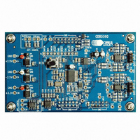
DEV BOARD FOR CS5560 W/MUX
Manufacturer
Cirrus Logic Inc
Type
A/Dr
Specifications of CDB5560
Number Of Adc's
1
Number Of Bits
24
Sampling Rate (per Second)
50k
Data Interface
Serial
Inputs Per Adc
1 Differential
Input Range
±3 V
Power (typ) @ Conditions
90mW @ 2.5 V
Voltage Supply Source
Dual ±
Operating Temperature
-40°C ~ 85°C
Utilized Ic / Part
CS5560
Product
Data Conversion Development Tools
Conversion Rate
50 KSPS
Resolution
24 bit
Maximum Clock Frequency
16 MHz
Interface Type
SPI
Supply Voltage (max)
3.3 V
Supply Voltage (min)
- 2.5 V
For Use With/related Products
CS5560
Lead Free Status / RoHS Status
Contains lead / RoHS non-compliant
Lead Free Status / RoHS Status
Lead free / RoHS Compliant, Contains lead / RoHS non-compliant
Other names
598-1273
CDB5560-1
CDB5560-1


For detailed information on the LMP7732 precision industrial op-amps, please visit National Semiconduc-
tor’s website at www.national.com.
The analog inputs are designed for connections to differential input signals. The usable input voltage
range is -4.096 V to +4.096 V. The theoretical input frequency range of the CS5560 is from DC to the
Nyquist frequency of 25 kHz. The analog input buffer amplifiers are configured for a cutoff frequency of
16.8 kHz to band-limit noise into the ADC. Changing the cutoff frequency will change the noise bandwidth
accordingly.
3.3.2
Analog input channel selection is controlled through the multiplexer. The multiplexer is configured with a
pull-down resistor on the MUX control line to enable input channel labeled "INPUT A" by default. To select
channel B, apply 3.3 V to the multiplexer input control line (MUX).
Signal levels for controlling the multiplexer that selects between analog input channels A and B is shown
in Table 3.
During multiplexing, the maximum sample rate for each channel is half that of the ADC’s maximum sam-
ple rate. Additionally, the Nyquist frequency for each channel is half of the ADC’s Nyquist frequency.
3.3.3
The CS5560 ADC makes use of an externally generated power-on reset. Therefore, after power is ap-
plied to the ADC, the reset pin must be driven low then released. Pressing the Reset button generates a
reset cycle. A reset cycle can be generated at any time during ADC operation. The ADC RST pin (active
low) is held inactive through a pull-up resistor.
3.3.4
The voltage reference IC provided generates a 4.096 V precision reference.
3.3.5
The reference frequency for the CS5560 ADC is provided by a 16.000 MHz oscillator.
DS713DB4
Multiplexer
ADC Reset
Voltage Reference
ADC Reference Frequency
Control Input (MUX)
Table 3. Analog Input Channel Selection
Multiplexer
3.3 V
0 V
Input Channel
Enabled
A
B
CDB5560
7
Related parts for CDB5560
Image
Part Number
Description
Manufacturer
Datasheet
Request
R

Part Number:
Description:
Development Kit
Manufacturer:
Cirrus Logic Inc
Datasheet:
Part Number:
Description:
Development Kit
Manufacturer:
Cirrus Logic Inc
Datasheet:


Part Number:
Description:
High-efficiency PFC + Fluorescent Lamp Driver Reference Design
Manufacturer:
Cirrus Logic Inc
Datasheet:
Part Number:
Description:
Development Kit
Manufacturer:
Cirrus Logic Inc
Datasheet:
Part Number:
Description:
Development Kit
Manufacturer:
Cirrus Logic Inc
Datasheet:

Part Number:
Description:
Development Kit
Manufacturer:
Cirrus Logic Inc
Datasheet:
Part Number:
Description:
Development Kit
Manufacturer:
Cirrus Logic Inc
Datasheet:
Part Number:
Description:
Development Kit
Manufacturer:
Cirrus Logic Inc
Datasheet:
Part Number:
Description:
Development Kit
Manufacturer:
Cirrus Logic Inc
Datasheet:

Part Number:
Description:
EVALUATION BOARD FOR CS8427
Manufacturer:
Cirrus Logic Inc
Datasheet:

Part Number:
Description:
BOARD EVAL FOR CS8416 RCVR
Manufacturer:
Cirrus Logic Inc
Datasheet:

Part Number:
Description:
EVALUATION BOARD FOR CS8420
Manufacturer:
Cirrus Logic Inc
Datasheet:

Part Number:
Description:
KIT DEVELOPMENT EP9315 ARM9
Manufacturer:
Cirrus Logic Inc
Datasheet:

Part Number:
Description:
KIT DEVELOPMENT EP9302 ARM9
Manufacturer:
Cirrus Logic Inc
Datasheet: