KDC5512H-Q48EVAL Intersil, KDC5512H-Q48EVAL Datasheet - Page 30
KDC5512H-Q48EVAL
Manufacturer Part Number
KDC5512H-Q48EVAL
Description
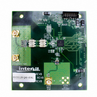
DAUGHTER CARD FOR KAD5512
Manufacturer
Intersil
Series
FemtoCharge™r
Datasheets
1.KAD5512HP-25Q72.pdf
(34 pages)
2.KMB-001LEVALZ.pdf
(7 pages)
3.KDC5514EVALZ.pdf
(9 pages)
Specifications of KDC5512H-Q48EVAL
Number Of Adc's
1
Number Of Bits
12
Sampling Rate (per Second)
250M
Data Interface
Parallel
Inputs Per Adc
1 Differential
Input Range
1.47 Vpp
Power (typ) @ Conditions
429mW @ 250MSPS
Voltage Supply Source
Single Supply
Operating Temperature
-40°C ~ 85°C
Utilized Ic / Part
KAD5512HP-25, KMB001 Motherboard
For Use With
KMB001LEVAL - MOTHERBOARD FOR LVDS ADC CARD
Lead Free Status / RoHS Status
Lead free / RoHS Compliant


INPUT
Equivalent Circuits
72 Pin/48 Pin Package Options
The KAD5512HP is available in both 72 pin and 48 pin
packages. The 48 pin package option supports LVDS DDR
only. A reduced set of pin selectable functions are available
in the 48 pin package due to the reduced pinout;
(OUTMODE, OUTFMT, and CLKDIV pins are not available).
Table 17 shows the default state for these functions for the
48 pin package. Note that these functions are available
through the SPI, allowing a user to set these modes as they
desire, offering the same flexibility as the 72 pin package
DATA
DATA
2mA OR
2mA OR
3mA
AVDD
3mA
FIGURE 43. TRI-LEVEL DIGITAL INPUTS
OVDD
280O Ω
FIGURE 45. LVDS OUTPUTS
75kO
75kO
Ω
Ω
AVDD
DATA
DATA
(Continued)
30
75kO
AVDD
Ω
OVDD
0.535V
OVDD
75kO
Ω
AVDD
+
–
FIGURE 47. VCM_OUT OUTPUT
D[11:0]P
D[11:0]N
SENSE
LOGIC
KAD5512HP
TO
option. DC and AC performance of the ADC is equivalent for
both package options.
.
FUNCTION
OUTMODE
OUTFMT
CLKDIV
TABLE 17. 48 PIN SPI - ADDRESSABLE FUNCTIONS
(20k PULL-UP
INPUT
ON RESETN
ONLY)
DATA
AVDD
OVDD
FIGURE 46. CMOS OUTPUTS
FIGURE 44. DIGITAL INPUTS
DESCRIPTION
Output Driver
Clock Divider
Data Coding
280Ω
VCM
OVDD
20kΩ
Mode
OVDD
OVDD
OVDD
Two’s Complement
LVDS, 3mA (DDR)
DEFAULT STATE
Divide by 1
D[11:0]
LOGIC
TO
October 1, 2009
FN6808.3
Related parts for KDC5512H-Q48EVAL
Image
Part Number
Description
Manufacturer
Datasheet
Request
R

Part Number:
Description:
DAUGHTER CARD FOR KDC5512
Manufacturer:
Intersil
Datasheet:

Part Number:
Description:
DAUGHTER CARD FOR KAD5512
Manufacturer:
Intersil
Datasheet:

Part Number:
Description:
DAUGHTER CARD FOR KAD5512
Manufacturer:
Intersil
Datasheet:

Part Number:
Description:
Intersil Corporation [CMOS Serial Controller Interface]
Manufacturer:
Intersil Corporation
Datasheet:
Part Number:
Description:
Manufacturer:
Intersil Corporation
Datasheet:
Part Number:
Description:
357-036-542-201 CARDEDGE 36POS DL .156 BLK LOPRO
Manufacturer:
Intersil Corporation
Datasheet:
Part Number:
Description:
1024-Word x 4-Bit LSI Static RAM
Manufacturer:
Intersil Corporation
Datasheet:
Part Number:
Description:
General Purpose NPN Transistor Arrays FN341.4
Manufacturer:
Intersil Corporation
Datasheet:
Part Number:
Description:
CMOS 16-Bit Microprocessor
Manufacturer:
Intersil Corporation
Datasheet:
Part Number:
Description:
Manufacturer:
Intersil Corporation
Datasheet:
Part Number:
Description:
Manufacturer:
Intersil Corporation
Datasheet:
Part Number:
Description:
Manufacturer:
Intersil Corporation
Datasheet:
Part Number:
Description:
Manufacturer:
Intersil Corporation
Datasheet:
Part Number:
Description:
CMOS 6-Bit Latch and Decoder Memory Interfaces
Manufacturer:
Intersil Corporation
Datasheet:
Part Number:
Description:
CA3046General Purpose NPN Transistor Arrays
Manufacturer:
Intersil Corporation
Datasheet: