KDC5512H-Q48EVAL Intersil, KDC5512H-Q48EVAL Datasheet - Page 3
KDC5512H-Q48EVAL
Manufacturer Part Number
KDC5512H-Q48EVAL
Description
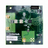
DAUGHTER CARD FOR KAD5512
Manufacturer
Intersil
Series
FemtoCharge™r
Datasheets
1.KAD5512HP-25Q72.pdf
(34 pages)
2.KMB-001LEVALZ.pdf
(7 pages)
3.KDC5514EVALZ.pdf
(9 pages)
Specifications of KDC5512H-Q48EVAL
Number Of Adc's
1
Number Of Bits
12
Sampling Rate (per Second)
250M
Data Interface
Parallel
Inputs Per Adc
1 Differential
Input Range
1.47 Vpp
Power (typ) @ Conditions
429mW @ 250MSPS
Voltage Supply Source
Single Supply
Operating Temperature
-40°C ~ 85°C
Utilized Ic / Part
KAD5512HP-25, KMB001 Motherboard
For Use With
KMB001LEVAL - MOTHERBOARD FOR LVDS ADC CARD
Lead Free Status / RoHS Status
Lead free / RoHS Compliant


Table of Contents
Absolute Maximum Ratings ......................................... 4
Thermal Information...................................................... 4
Operating Conditions.................................................... 4
Electrical Specifications ............................................... 4
Digital Specifications .................................................... 6
Timing Diagrams ........................................................... 7
Switching Specifications .............................................. 8
Pinout/Package Information......................................... 9
Typical Performance Curves ........................................ 14
Theory of Operation ...................................................... 17
Pin Descriptions - 72QFN........................................... 9
Pinout ......................................................................... 11
Pin Descriptions - 48QFN........................................... 12
Pinout ......................................................................... 13
Functional Description ................................................ 17
Power-On Calibration ................................................. 17
User-Initiated Reset.................................................... 18
Analog Input ............................................................... 18
Clock Input ................................................................. 19
Jitter............................................................................ 20
Voltage Reference...................................................... 20
Digital Outputs ............................................................ 20
Over-Range Indicator ................................................. 20
Power Dissipation....................................................... 20
Nap/Sleep................................................................... 21
Data Format ............................................................... 21
3
KAD5512HP
Serial Peripheral Interface ........................................... 22
Equivalent Circuits ....................................................... 29
72 Pin/48 Pin Package Options ................................... 30
ADC Evaluation Platform ............................................. 31
Layout Considerations................................................. 31
Definitions ..................................................................... 31
Revision History ........................................................... 32
Package Outline Drawings........................................... 33
SPI Physical Interface................................................ 23
SPI Configuration....................................................... 24
Device Information ..................................................... 24
Indexed Device Configuration/Control ....................... 24
Global Device Configuration/Control.......................... 25
Device Test ................................................................ 27
SPI Memory Map ....................................................... 28
Split Ground and Power Planes................................. 31
Clock Input Considerations ........................................ 31
Exposed Paddle......................................................... 31
Bypass and Filtering .................................................. 31
LVDS Outputs ............................................................ 31
LVCMOS Outputs ...................................................... 31
Unused Inputs............................................................ 31
L48.7x7E.................................................................... . 33
L72.10x10D................................................................ . 34
October 1, 2009
FN6808.3
Related parts for KDC5512H-Q48EVAL
Image
Part Number
Description
Manufacturer
Datasheet
Request
R

Part Number:
Description:
DAUGHTER CARD FOR KDC5512
Manufacturer:
Intersil
Datasheet:

Part Number:
Description:
DAUGHTER CARD FOR KAD5512
Manufacturer:
Intersil
Datasheet:

Part Number:
Description:
DAUGHTER CARD FOR KAD5512
Manufacturer:
Intersil
Datasheet:

Part Number:
Description:
Intersil Corporation [CMOS Serial Controller Interface]
Manufacturer:
Intersil Corporation
Datasheet:
Part Number:
Description:
Manufacturer:
Intersil Corporation
Datasheet:
Part Number:
Description:
357-036-542-201 CARDEDGE 36POS DL .156 BLK LOPRO
Manufacturer:
Intersil Corporation
Datasheet:
Part Number:
Description:
1024-Word x 4-Bit LSI Static RAM
Manufacturer:
Intersil Corporation
Datasheet:
Part Number:
Description:
General Purpose NPN Transistor Arrays FN341.4
Manufacturer:
Intersil Corporation
Datasheet:
Part Number:
Description:
CMOS 16-Bit Microprocessor
Manufacturer:
Intersil Corporation
Datasheet:
Part Number:
Description:
Manufacturer:
Intersil Corporation
Datasheet:
Part Number:
Description:
Manufacturer:
Intersil Corporation
Datasheet:
Part Number:
Description:
Manufacturer:
Intersil Corporation
Datasheet:
Part Number:
Description:
Manufacturer:
Intersil Corporation
Datasheet:
Part Number:
Description:
CMOS 6-Bit Latch and Decoder Memory Interfaces
Manufacturer:
Intersil Corporation
Datasheet:
Part Number:
Description:
CA3046General Purpose NPN Transistor Arrays
Manufacturer:
Intersil Corporation
Datasheet: