KDC5512H-Q48EVAL Intersil, KDC5512H-Q48EVAL Datasheet
KDC5512H-Q48EVAL
Specifications of KDC5512H-Q48EVAL


Related parts for KDC5512H-Q48EVAL


KDC5512H-Q48EVAL Summary of contents
Page 1
... KAD5512P-25, KAD5512HP-25 KAD5512P-21, KAD5512HP-21 KAD5512P-17, KAD5512HP-17 KAD5512P-12, KAD5512HP-12 KAD5510P-50 CAUTION: These devices are sensitive to electrostatic discharge; follow proper IC Handling Procedures. 1-888-INTERSIL or 1-888-468-3774 FemtoCharge is a trademark of Kenet Inc. Copyright Intersil Americas Inc. 2008, 2009. All Rights Reserved KAD5512HP October 1, 2009 MODEL RESOLUTION ...
Page 2
... These Intersil Pb-free plastic packaged products employ special Pb-free material sets, molding compounds/die attach materials, and 100% matte tin plate plus anneal (e3 termination finish, which is RoHS compliant and compatible with both SnPb and Pb-free soldering operations). Intersil Pb-free products are MSL classified at Pb-free peak reflow temperatures that meet or exceed the Pb-free requirements of IPC/JEDEC J STD- ...
Page 3
Table of Contents Absolute Maximum Ratings ......................................... 4 Thermal Information...................................................... 4 Operating Conditions.................................................... 4 Electrical Specifications ............................................... 4 Digital Specifications .................................................... 6 Timing Diagrams ........................................................... 7 Switching Specifications .............................................. 8 Pinout/Package Information......................................... 9 Pin Descriptions - 72QFN........................................... 9 Pinout ......................................................................... ...
Page 4
... KAD5512HP Thermal Information Thermal Resistance (Typical, Note QFN . . . . . . . . . . . . . . . . . . . . . . . . . . . . . . . . 72 Ld QFN . . . . . . . . . . . . . . . . . . . . . . . . . . . . . . . . Storage Temperature . . . . . . . . . . . . . . . . . . . . . . . .-65°C to +150°C Junction Temperature . . . . . . . . . . . . . . . . . . . . . . . . . . . . . . +150°C Pb-Free Reflow Profile .see link below http://www.intersil.com/pbfree/Pb-FreeReflow.asp Operating Conditions Temperature Range . . . . . . . . . . . . . . . . . . . . . . . . . .-40°C to +85°C = -1dBFS KAD5512HP-25 KAD5512HP-21 (Note 4) (Note 4) MIN ...
Page 5
Electrical Specifications All specifications apply under the following conditions unless otherwise noted: AVDD = 1.8V, OVDD = 1.8V -40°C to +85°C (typical specifications at +25°C (per speed grade). (Continued) PARAMETER SYMBOL CONDITIONS 1.8V Digital Supply I ...
Page 6
Electrical Specifications All specifications apply under the following conditions unless otherwise noted: AVDD = 1.8V, OVDD = 1.8V -40°C to +85°C (typical specifications at +25°C (per speed grade). (Continued) PARAMETER SYMBOL CONDITIONS Spurious-Free SFDR f = ...
Page 7
Digital Specifications (Continued) PARAMETER SYMBOL LVDS OUTPUTS Differential Output Voltage Output Offset Voltage Output Rise Time Output Fall Time CMOS OUTPUTS Voltage Output High Voltage Output Low Output Rise Time Output Fall Time Timing Diagrams SAMPLE N INP INN t ...
Page 8
Switching Specifications PARAMETER ADC OUTPUT Aperture Delay RMS Aperture Jitter Output Clock to Data Propagation Delay, LVDS Mode (Note 9) Output Clock to Data Propagation Delay, CMOS Mode (Note 9) Latency (Pipeline Delay) Overvoltage Recovery SPI INTERFACE (Notes 10, 11) ...
Page 9
Pinout/Package Information Pin Descriptions - 72QFN PIN NUMBER LVDS [LVCMOS] NAME 1, 6, 12, 19, 24, 71 AVDD 2-5, 13, 14, 17, 18, 28-31 DNC 7, 8, 11, 72 AVSS 9, 10 VINN, VINP 15 VCM 16 CLKDIV 20, 21 ...
Page 10
Pin Descriptions - 72QFN (Continued) PIN NUMBER LVDS [LVCMOS] NAME 46 RLVDS 47 CLKOUTN [NC] 48 CLKOUTP [CLKOUT] 49 D6N [NC] 50 D6P [D6] 51 D7N [NC] 52 D7P [D7] 53 D8N [NC] 54 D8P [D8] 57 D9N [NC] 58 ...
Page 11
Pinout AVDD 1 DNC 2 DNC 3 4 DNC 5 DNC 6 AVDD 7 AVSS AVSS 8 9 VINN 10 VINP 11 AVSS 12 AVDD 13 DNC 14 DNC 15 VCM 16 CLKDIV 17 DNC DNC 18 ...
Page 12
Pin Descriptions - 48QFN PIN NUMBER 1, 9, 13, 17, 47 2-4, 11 19, 29 ...
Page 13
Pin Descriptions - 48QFN (Continued) PIN NUMBER Exposed Paddle NOTE: LVCMOS Output Mode Functionality is shown in brackets ( Connection) Pinout AVDD 1 DNC 2 3 DNC DNC 4 AVSS 5 6 VINN 7 ...
Page 14
Typical Performance Curves 90 SFDR @ 250MSPS 85 80 SFDR @ 125MSPS 75 SNR @ 125MSPS SNR @ 250MSPS 200M 400M INPUT FREQUENCY (Hz) FIGURE 3. SNR AND SFDR vs f 100 90 80 ...
Page 15
Typical Performance Curves 450 400 SDR 350 300 250 200 150 100 40 70 100 130 160 SAMPLE RATE (MSPS) FIGURE 9. POWER 3mA LVDS MODE SAMPLE 1.0 0.8 0.6 0.4 0.2 0.0 -0.2 -0.4 -0.6 -0.8 ...
Page 16
Typical Performance Curves 0 Ain = -1.0dBFS SNR = 68.0dBFS -20 SFDR = 82.6dBc SINAD = 67.8dBFS -40 -60 -80 -100 -120 0M 20M 40M 60M FREQUENCY (Hz) FIGURE 15. SINGLE-TONE SPECTRUM @ 105MHz 0 -20 -40 -60 -80 -100 ...
Page 17
Theory of Operation Functional Description The KAD5512HP is based upon a 12-bit, 250MSPS A/D converter core that utilizes a pipelined successive approximation architecture (Figure 21). The input voltage is captured by a Sample-Hold Amplifier (SHA) and converted to a unit ...
Page 18
The calibration sequence is initiated on the rising edge of RESETN, as shown in Figure 22. The over-range output (OR) is set high once RESETN is pulled low, and remains in that state until calibration is complete. The OR output ...
Page 19
VCM voltage of 0.535V as shown in Figure 25. 1.8 1.4 INP 1.0 0.725V 0.6 0.2 FIGURE 25. ANALOG INPUT RANGE Best performance is obtained when the analog inputs are driven differentially. ...
Page 20
The clock divider can also be controlled through the SPI port, which overrides the CLKDIV pin setting. Details on this are contained in “Serial Peripheral Interface” on page 22. A delay-locked loop (DLL) generates internal clock signals for various stages ...
Page 21
Nap/Sleep Portions of the device may be shut down to save power during times when operation of the ADC is not required. Two power saving modes are available: Nap, and Sleep. Nap mode reduces power dissipation to less than 163mW ...
Page 22
GRAY CODE BINARY FIGURE 32. GRAY CODE TO BINARY CONVERSION Mapping of the input voltage to the various data formats is shown in Table 5. TABLE 5. INPUT VOLTAGE TO OUTPUT CODE MAPPING INPUT ...
Page 23
DSW CSB t S SCLK SDIO R DSW CSB t S SCLK SDIO R SDO CSB SCLK SDIO INSTRUCTION/ADDRESS CSB SCLK SDIO INSTRUCTION/ADDRESS SPI Physical Interface The serial clock pin (SCLK) provides synchronization for ...
Page 24
... A common SPI map, which can accommodate 3 single-channel or multi-channel devices, is used for all Intersil ADC products. Certain configuration commands 4 or more (identified as Indexed in the SPI map) can be executed on a per-converter basis. This register determines which converter is being addressed for an Indexed command important to note that only a single converter can be addressed at a time ...
Page 25
ADDRESS 0X20: OFFSET_COARSE ADDRESS 0X21: OFFSET_FINE The input offset of each ADC core can be adjusted in fine and coarse steps. Both adjustments are made via an 8-bit word as detailed in ...
Page 26
ADDRESS 0X72: CLOCK_DIVIDE The KAD5512HP has a selectable clock divider that can be set to divide by four, two or one (no division). By default, the tri-level CLKDIV pin selects the divisor (refer to “Clock Input Considerations” on page 31). ...
Page 27
Device Test The KAD5512HP can produce preset or user defined patterns on the digital outputs to facilitate in-situ testing. A static word can be placed on the output bus, or two different words can alternate. In the alternate mode, the ...
Page 28
SPI Memory Map ADDR PARAMETER BIT 7 (Hex) NAME (MSB) 00 Port_Config SDO Active 01 Reserved 02 Burst_End 03-07 Reserved 08 Chip_Id 09 Chip_Version 10 Device_Index_A 11-1F Reserved 20 Offset_Coarse 21 Offset_Fine 22 Gain_Coarse 23 Gain_Medium 24 Gain_Fine 25 Modes ...
Page 29
ADDR PARAMETER BIT 7 (Hex) NAME (MSB) C0 Test_io User Test Mode 00 = Single 01 = Alternate 10 = Reserved 11 = Reserved C1 Reserved C2 User_Patt 1_LSB B7 C3 User_Patt1_MSB B15 C4 User_Patt 2_LSB B7 C5 User_Patt2_MSB B15 ...
Page 30
Equivalent Circuits (Continued) AVDD AVDD Ω 75kO AVDD Ω 75kO 280O Ω INPUT Ω 75kO FIGURE 43. TRI-LEVEL DIGITAL INPUTS OVDD 2mA OR 3mA DATA DATA OVDD DATA DATA 2mA OR 3mA FIGURE 45. LVDS OUTPUTS 0.535V 72 Pin/48 Pin ...
Page 31
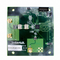
... ADC Evaluation Platform Intersil offers an ADC Evaluation platform which can be used to evaluate any of the KADxxxxx ADC family. The platform consists of a FPGA based data capture motherboard and a family of ADC daughtercards. This USB based platform allows a user to quickly evaluate the ADC’s performance at a user’ ...
Page 32
... Accordingly, the reader is cautioned to verify that data sheets are current before placing orders. Information furnished by Intersil is believed to be accurate and reliable. However, no responsibility is assumed by Intersil or its subsidiaries for its use; nor for any infringements of patents or other rights of third parties which may result from its use ...
Page 33
Package Outline Drawing L48.7x7E 48 LEAD QUAD FLAT NO-LEAD PLASTIC PACKAGE Rev 1, 2/09 7.00 PIN 1 INDEX AREA 6 (4X) 0.15 TOP VIEW 6.80 Sq 5.60 Sq TYPICAL RECOMMENDED LAND PATTERN 33 KAD5512HP Exp. DAP ...
Page 34
Package Outline Drawing L72.10x10D 72 LEAD QUAD FLAT NO-LEAD PLASTIC PACKAGE Rev 1, 11/08 10.00 PIN 1 INDEX AREA 6 (4X) 0.15 TOP VIEW 9.80 Sq 6.00 Sq TYPICAL RECOMMENDED LAND PATTERN 34 KAD5512HP 10.00 37 ...