CDB5345 Cirrus Logic Inc, CDB5345 Datasheet - Page 8
CDB5345
Manufacturer Part Number
CDB5345
Description
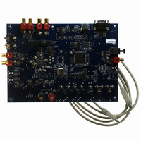
EVALUATION BOARD FOR CS5345
Manufacturer
Cirrus Logic Inc
Specifications of CDB5345
Number Of Adc's
2
Number Of Bits
24
Sampling Rate (per Second)
192k
Data Interface
Serial
Inputs Per Adc
6 Single Ended
Power (typ) @ Conditions
400mW @ 5 V
Voltage Supply Source
Analog and Digital
Operating Temperature
-10°C ~ 70°C
Utilized Ic / Part
CS5345
Description/function
Audio A/D
Operating Supply Voltage
5 V
Product
Audio Modules
For Use With/related Products
CS5345
Lead Free Status / RoHS Status
Contains lead / RoHS non-compliant
Lead Free Status / RoHS Status
Lead free / RoHS Compliant, Contains lead / RoHS non-compliant
Other names
598-1780


3.2
3.3
8
Register Maps Tab
The Register Maps tab provides low level control over the register level settings of the CS5345, CS8406,
and FPGA. Each device is displayed on a separate tab. Register values can be modified bit-wise or byte-
wise. For bit-wise, click the appropriate push button for the desired bit. For byte-wise, the desired hex value
can be typed directly in the register address box in the register map.
Pre-Configured Script Files
Pre-configured script files are provided with the CDB5345 to allow easy initial board bring-up. The board
configurations stored within these files are described in sections 3.3.1 - 3.3.2.
3.3.1
Using the pre-configured script file named “Oscillator Clock - ADC Ch 1 In to SPDIF & PGA Out.txt”, an an-
alog input signal applied to channel 1 of the CS5345 input multiplexer will be digitized by the ADC, transmit-
ted in S/PDIF format by the CS8406, and will be output through the active output filter and RCA jacks.
The canned oscillator is the source of MCLK. The CS5345 is the sub-clock master to the CS8406 and the
PCM1I/O header.
Oscillator Clock - ADC Ch 1 In to In to SPDIF & PGA Out
Figure 2. Register Maps Tab
CDB5345
DS658DB1
Related parts for CDB5345
Image
Part Number
Description
Manufacturer
Datasheet
Request
R

Part Number:
Description:
Development Kit
Manufacturer:
Cirrus Logic Inc
Datasheet:
Part Number:
Description:
Development Kit
Manufacturer:
Cirrus Logic Inc
Datasheet:


Part Number:
Description:
High-efficiency PFC + Fluorescent Lamp Driver Reference Design
Manufacturer:
Cirrus Logic Inc
Datasheet:
Part Number:
Description:
Development Kit
Manufacturer:
Cirrus Logic Inc
Datasheet:
Part Number:
Description:
Development Kit
Manufacturer:
Cirrus Logic Inc
Datasheet:

Part Number:
Description:
Development Kit
Manufacturer:
Cirrus Logic Inc
Datasheet:
Part Number:
Description:
Development Kit
Manufacturer:
Cirrus Logic Inc
Datasheet:
Part Number:
Description:
Development Kit
Manufacturer:
Cirrus Logic Inc
Datasheet:
Part Number:
Description:
Development Kit
Manufacturer:
Cirrus Logic Inc
Datasheet:

Part Number:
Description:
EVALUATION BOARD FOR CS8427
Manufacturer:
Cirrus Logic Inc
Datasheet:

Part Number:
Description:
BOARD EVAL FOR CS8416 RCVR
Manufacturer:
Cirrus Logic Inc
Datasheet:

Part Number:
Description:
EVALUATION BOARD FOR CS8420
Manufacturer:
Cirrus Logic Inc
Datasheet:

Part Number:
Description:
KIT DEVELOPMENT EP9315 ARM9
Manufacturer:
Cirrus Logic Inc
Datasheet:

Part Number:
Description:
KIT DEVELOPMENT EP9302 ARM9
Manufacturer:
Cirrus Logic Inc
Datasheet: