CDB5345 Cirrus Logic Inc, CDB5345 Datasheet
CDB5345
Specifications of CDB5345


Related parts for CDB5345


CDB5345 Summary of contents
Page 1
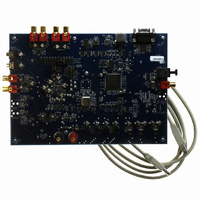
... Microphone Input Control Port Interface Cirrus Logic, Inc. www.cirrus.com Description The CDB5345 evaluation board is an excellent means for evaluating the CS5345 ADC. Evaluation requires an analog signal source and analog/digital analyzer, and power supplies. A Windows must be used to evaluate the CS5345. System timing for the I²S, Left-Justified and Right-Justi- ...
Page 2
... USB Control Port ............................................................................................................. 5 2. SYSTEM CLOCKS AND DATA ................................................................................................ 6 2.1 Clock Routing ..................................................................................................................... 6 2.2 Data Routing ...................................................................................................................... SOFTWARE CONTROL ..................................................................................................... 7 3.1 CDB5345 Controls Tab ...................................................................................................... 7 3.2 Register Maps Tab ............................................................................................................. 8 3.3 Pre-Configured Script Files ................................................................................................ 8 3.3.1 Oscillator Clock - ADC SPDIF & PGA Out ................................... 8 3.3.2 Oscillator Clock - ADC SPDIF Out ............................................... 9 4 ...
Page 3
... LIST OF FIGURES Figure 1. CDB5345 Controls Tab.................................................................................................... 7 Figure 2. Register Maps Tab........................................................................................................... 8 Figure 3. Block Diagram................................................................................................................ 15 Figure 4. CS5345 .......................................................................................................................... 16 Figure 5. Analog Inputs ................................................................................................................. 17 Figure 6. Analog Outputs .............................................................................................................. 18 Figure 7. S/PDIF Output................................................................................................................ 19 Figure 8. Control Port.................................................................................................................... 20 Figure 9. FPGA ............................................................................................................................. 21 Figure 10. Discrete Clock Routing and Level Shifting................................................................... 22 Figure 11. Power........................................................................................................................... 23 Figure 12. Silk Screen................................................................................................................... 24 Figure 13 ...
Page 4
... The FPGA handles both clock and data routing on the CDB5345. Clock and data routing selections made via the CDB5345 Controls tab in the GUI will be handled by the FPGA with no user intervention required. For advanced information regarding the internal registers and operation of the FPGA, see sections 4 and 5 beginning on page 10 ...
Page 5
... RCA jacks for easy evaluation. 1.10 Serial Control Port A graphical user interface is included with the CDB5345 to allow easy manipulation of the registers in the CS5345, CS8406, and FPGA. See the device-specific data sheets for the CS5345 and CD8406 internal reg- ister descriptions. The internal register map for the FPGA is located in section 4 on page 10. ...
Page 6
... SYSTEM CLOCKS AND DATA The CDB5345 implements comprehensive clock routing capabilities. Configuration of the clock routing can be easily achieved using the controls within the Board Controls group box on the CDB5345 Controls tab in the GUI software application. 2.1 Clock Routing The master clock signal (MCLK) may be sourced from the canned oscillator (Y1) or the PCM1 I/O header ...
Page 7
... The CDB5345 Controls tab provides a high-level intuitive interface to many of the configuration options of the CS5345 and CDB5345. The controls within the ADC/PGA Controls group box control the internal regis- ters of the CS5345. The controls within the Board Controls group box control the board level clock and data routing on the CDB5345 ...
Page 8
... Pre-Configured Script Files Pre-configured script files are provided with the CDB5345 to allow easy initial board bring-up. The board configurations stored within these files are described in sections 3.3.1 - 3.3.2. 3.3.1 Oscillator Clock - ADC SPDIF & PGA Out Using the pre-configured script file named “ ...
Page 9
... CS5345 input multiplexer will be digitized by the ADC and transmitted in S/PDIF format by the CS8406. No signal will be output through the active output filter and RCA jacks. The canned oscillator is the source of MCLK. The CS5345 is the sub-clock master to the CS8406 and the PCM1I/O header. DS658DB1 CDB5345 9 ...
Page 10
... Reserved Reserved 0 05h Transmitter Reserved Reserved SDIN Source Rev6 Rev5 Rev4 Reserved Reserved Reserved Reserved Reserved Reserved Reserved Reserved Reserved Reserved CS8406 Reserved CDB5345 Rev3 Rev2 Rev1 Reserved Reserved Reserved SUBCLK1 Reserved Reserved Reserved Reserved DS658DB1 0 Rev0 x MCLK 0 SUBCLK0 1 Reserved 0 Reserved ...
Page 11
... Default = 0 Function: This bit selects the source of the CS5345 MCLK signal. Table 1 shows the available settings. MCLK 0 1 DS658DB1 Rev4 Rev3 Reserved Reserved Table 1. MCLK Source MCLK Source Canned Oscillator M1 position on PCM1 I/O Header CDB5345 Rev2 Rev1 Rev0 Reserved Reserved MCLK 11 ...
Page 12
... PCM I/O Header Subclocks are Output from CS8406 0 - CS5345 is Slave to Header - CS8406 is Slave to Header - PCM I/O Header Subclocks are an Input CS8406 Reserved Table 3. CS8406 SDIN Source CS8406 SDIN Source Reserved CS5345 SDOUT CDB5345 2 1 Reserved SUBCLK1 SUBCLK0 Reserved 2 1 Reserved Reserved 0 0 Reserved DS658DB1 ...
Page 13
... RCA phono jacks for analog input signal to CS5345. Active Input input buffer. 1/8“ TRS jacks for microphone input. Input RCA phono jacks for PGA analog outputs. Active output Output buffer. Table 4. System Connections CDB5345 SIGNAL PRESENT 2 C control port signals 2 C control port signals control port signals. 13 ...
Page 14
... V* Select RCA input multiplexer as source. Line Input* Select TRS inputs as source. Mic Input Passive filter mapped to input MUX channel. Passive Filter* Active filter mapped to input MUX channel. Active Filter *Default factory settings Table 5. System Jumper Settings CDB5345 FUNCTION SELECTED DS658DB1 ...
Page 15
... CDB BLOCK DIAGRAM DS658DB1 CDB5345 15 ...
Page 16
... CDB SCHEMATICS 16 CDB5345 DS658DB1 ...
Page 17
... DS658DB1 CDB5345 17 ...
Page 18
... CDB5345 DS658DB1 ...
Page 19
... DS658DB1 CDB5345 19 ...
Page 20
... CDB5345 DS658DB1 ...
Page 21
... DS658DB1 CDB5345 21 ...
Page 22
... CDB5345 DS658DB1 ...
Page 23
... DS658DB1 CDB5345 23 ...
Page 24
... CDB LAYOUT 24 CDB5345 DS658DB1 ...
Page 25
... DS658DB1 CDB5345 25 ...
Page 26
... CDB5345 DS658DB1 ...
Page 27
... Cirrus Logic, Cirrus, the Cirrus Logic logo designs, and Popguard are trademarks of Cirrus Logic, Inc. All other brand and product names in this doc- ument may be trademarks or service marks of their respective owners. Windows is a registered trademark of Microsoft Corporation. DS658DB1 Initial Release Table 6. Revision History CDB5345 Changes 27 ...