EVAL-AD7991EBZ Analog Devices Inc, EVAL-AD7991EBZ Datasheet - Page 24
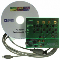
EVAL-AD7991EBZ
Manufacturer Part Number
EVAL-AD7991EBZ
Description
BOARD EVAL FOR AD7991
Manufacturer
Analog Devices Inc
Specifications of EVAL-AD7991EBZ
Number Of Adc's
1
Number Of Bits
12
Sampling Rate (per Second)
1M
Data Interface
Serial
Inputs Per Adc
4 Single Ended
Input Range
0 ~ Vdd
Power (typ) @ Conditions
4.4mW @ 5.5 V, 3.4MHz
Voltage Supply Source
Single Supply
Operating Temperature
-40°C ~ 125°C
Utilized Ic / Part
AD7991
Silicon Manufacturer
Analog Devices
Application Sub Type
ADC
Kit Application Type
Data Converter
Silicon Core Number
AD7991
Kit Contents
Board
Rohs Compliant
Yes
Lead Free Status / RoHS Status
Lead free / RoHS Compliant


AD7991/AD7995/AD7999
READING FROM THE AD7991/AD7995/AD7999
Reading data from the conversion result register is a 2-byte
operation, as shown in Figure 25. Therefore, a read operation
always involves two bytes.
After the AD7991/AD7995/AD7999 have received a read
address, any number of reads can be performed from the
conversion result register.
Following a start condition, the master writes the 7-bit address
of the AD7991/AD7995/AD7999 and then sets R/ W to 1. The
AD7991/AD7995/AD7999 acknowledge this by pulling the
SDA line low. They then output the conversion result over the
I
leading 0s followed by the channel identifier bits. For the
AD7995 there are two trailing 0s, and for the AD7999 there are
four trailing 0s.
After the master has addressed the AD7991/AD7995/AD7999,
the part begins to power up on the ninth SCLK rising edge. At
the same time, the acquisition phase begins. When approximately
0.6 μs have elapsed, the acquisition phase ends. The input is
sampled and a conversion begins. This is done in parallel to the
2
SDA
SCL
C bus, preceded by four status bits. The status bits are two
START BY
MASTER
0
1
1
SERIAL BUS ADDRESS BYTE
0
1
FRAME 1
Figure 25. Reading Two Bytes of Data from the AD7991Conversion Result Register
0
SCL (CONTINUED)
SDA (CONTINUED)
0
A0
R/W
ACK BY
Rev. B | Page 24 of 28
ADC
9
D7
1
0
1
read operation and should not affect the read operation. The
master reads back two bytes of data. On the ninth SCLK rising
edge of the second byte, if the master sends an ACK, it keeps
reading conversion results and the AD7991/AD7995/AD7999
powers up and performs a second conversion. If the master sends
a NO ACK, the AD7991/AD7995/AD7999 does not power up
on the ninth SCLK rising edge of the second byte. If a further
conversion is required, the part converts on the next channel, as
selected in the configuration register. See Table 11 for information
about the channel selection.
If the master sends a NO ACK on the ninth SCLK rising edge of
the second byte, the conversion is finished and no further
conversion is preformed.
To put the part into full shutdown mode, the user should issue a
stop condition to the AD7991/AD7995/AD7999. If the AD7991/
AD7995/AD7999 is not put into full shutdown mode, it will draw
a few tens of microamperes from the supply.
D6
LEAST SIGNIFICANT DATA BYTE FROM ADC
0
MOST SIGNIFICANT DATA BYTE FROM ADC
CH
D5
ID1
CH
D4
ID0
FRAME 2
FRAME 3
D11
D3
D10
D2
D1
D9
D8
D0
NO ACK BY
MASTER
MASTER
ACK BY
9
9
STOP BY
MASTER
Related parts for EVAL-AD7991EBZ
Image
Part Number
Description
Manufacturer
Datasheet
Request
R


Part Number:
Description:
BOARD EVAL FOR SI270X-A
Manufacturer:
Silicon Laboratories Inc
Datasheet:

Part Number:
Description:
BUCK CONV REF DESIGN KIT IP1201
Manufacturer:
International Rectifier
Datasheet:
Part Number:
Description:
BOARD DEMO SYNC DUAL BUCK CNVTER
Manufacturer:
International Rectifier
Datasheet:
Part Number:
Description:
BOARD DEMO SYNC BUCK CONVETER
Manufacturer:
International Rectifier
Datasheet:

Part Number:
Description:
EVALBOARD/EB Omnidirectional microphone - Analog
Manufacturer:
Analog Devices
Datasheet:
Part Number:
Description:
EVALBOARD/EB Omnidirectional microphone - Analog
Manufacturer:
Analog Devices
Datasheet:


Part Number:
Description:
BOARD EVAL LED DRIVER LT3756
Manufacturer:
Linear Technology
Datasheet:

Part Number:
Description:
BOARD EVAL FOR AD7741/7742
Manufacturer:
Analog Devices Inc
Datasheet:

Part Number:
Description:
±1.7g Dual-Axis IMEMS Accelerometer Evaluation Board
Manufacturer:
Analog Devices Inc
Datasheet:

Part Number:
Description:
IC MULTIPLIER ANALOG 8-SOIC T/R
Manufacturer:
Analog Devices Inc
Datasheet:

Part Number:
Description:
IC ANALOG MULTIPLIER 8-DIP
Manufacturer:
Analog Devices Inc
Datasheet:
Part Number:
Description:
IC ANALOG MULTIPLIER 8-SOIC
Manufacturer:
Analog Devices Inc
Datasheet:
Part Number:
Description:
IC ANALOG MULTIPLIER 8-DIP
Manufacturer:
Analog Devices Inc
Datasheet: