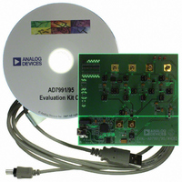
EVAL-AD7991EBZ Analog Devices Inc, EVAL-AD7991EBZ Datasheet - Page 22
EVAL-AD7991EBZ
Manufacturer Part Number
EVAL-AD7991EBZ
Description
BOARD EVAL FOR AD7991
Manufacturer
Analog Devices Inc
Specifications of EVAL-AD7991EBZ
Number Of Adc's
1
Number Of Bits
12
Sampling Rate (per Second)
1M
Data Interface
Serial
Inputs Per Adc
4 Single Ended
Input Range
0 ~ Vdd
Power (typ) @ Conditions
4.4mW @ 5.5 V, 3.4MHz
Voltage Supply Source
Single Supply
Operating Temperature
-40°C ~ 125°C
Utilized Ic / Part
AD7991
Silicon Manufacturer
Analog Devices
Application Sub Type
ADC
Kit Application Type
Data Converter
Silicon Core Number
AD7991
Kit Contents
Board
Rohs Compliant
Yes
Lead Free Status / RoHS Status
Lead free / RoHS Compliant


AD7991/AD7995/AD7999
SERIAL INTERFACE
Control of the AD7991/AD7995/AD7999 is accomplished via
the I
connected to this bus as a slave device under the control of a
master device, such as the processor.
SERIAL BUS ADDRESS
Like all I
a 7-bit serial address. The devices are available in two versions, the
AD7991-0/AD7995-0 and the AD7991-1/AD7995-1/AD7999-1.
Each version has a different address (see Table 8), which allows up
to two AD7991/AD7995 devices to be connected to a single
serial bus. AD7999 has only one version.
The serial bus protocol operates as follows:
1.
2.
3.
2
The master initiates a data transfer by establishing a start
condition, defined as a high-to-low transition on the serial
data line SDA while the serial clock line, SCL, remains high.
This indicates that an address/data stream follows.
All slave peripherals connected to the serial bus respond to
the start condition and shift in the next eight bits, consisting of
a 7-bit address (MSB first) plus an R/ W bit that determines
the direction of the data transfer—that is, whether data is
written to or read from the slave device.
The peripheral whose address corresponds to the transmitted
address responds by pulling the data line low during the
low period before the ninth clock pulse, known as the
acknowledge bit. All other devices on the bus remain idle
while the selected device waits for data to be read from or
written to it. If the R/ W bit is set to 0, the master writes to
the slave device. If the R/ W bit is set to 1, the master reads
from the slave device.
C-compatible serial bus. The AD7991/AD7995/AD7999 is
2
C-compatible devices, the AD7991/AD7995/AD7999 has
Rev. B | Page 22 of 28
4.
5.
6.
Data is sent over the serial bus in sequences of nine clock
pulses—eight bits of data followed by an acknowledge bit
from the receiver of data. Transitions on the data line must
occur during the low period of the clock signal and remain
stable during the high period because a low-to-high transition
when the clock is high may be interpreted as a stop signal.
When all data bytes have been read or written, stop conditions
are established. In write mode, the master pulls the data line
high during the 10
In read mode, the master device pulls the data line high
during the low period before the ninth clock pulse. This is
known as a no acknowledge. The master takes the data line
low during the low period before the 10
then high during the 10
Any number of bytes of data can be transferred over the serial
bus in one operation, but it is not possible to mix reads and
writes in one operation because the type of operation is
determined at the beginning and cannot subsequently be
changed without starting a new operation.
th
clock pulse to assert a stop condition.
th
clock pulse to assert a stop condition.
th
clock pulse, and
Related parts for EVAL-AD7991EBZ
Image
Part Number
Description
Manufacturer
Datasheet
Request
R


Part Number:
Description:
BOARD EVAL FOR SI270X-A
Manufacturer:
Silicon Laboratories Inc
Datasheet:

Part Number:
Description:
BUCK CONV REF DESIGN KIT IP1201
Manufacturer:
International Rectifier
Datasheet:
Part Number:
Description:
BOARD DEMO SYNC DUAL BUCK CNVTER
Manufacturer:
International Rectifier
Datasheet:
Part Number:
Description:
BOARD DEMO SYNC BUCK CONVETER
Manufacturer:
International Rectifier
Datasheet:

Part Number:
Description:
EVALBOARD/EB Omnidirectional microphone - Analog
Manufacturer:
Analog Devices
Datasheet:
Part Number:
Description:
EVALBOARD/EB Omnidirectional microphone - Analog
Manufacturer:
Analog Devices
Datasheet:


Part Number:
Description:
BOARD EVAL LED DRIVER LT3756
Manufacturer:
Linear Technology
Datasheet:

Part Number:
Description:
BOARD EVAL FOR AD7741/7742
Manufacturer:
Analog Devices Inc
Datasheet:

Part Number:
Description:
±1.7g Dual-Axis IMEMS Accelerometer Evaluation Board
Manufacturer:
Analog Devices Inc
Datasheet:

Part Number:
Description:
IC MULTIPLIER ANALOG 8-SOIC T/R
Manufacturer:
Analog Devices Inc
Datasheet:

Part Number:
Description:
IC ANALOG MULTIPLIER 8-DIP
Manufacturer:
Analog Devices Inc
Datasheet:
Part Number:
Description:
IC ANALOG MULTIPLIER 8-SOIC
Manufacturer:
Analog Devices Inc
Datasheet:
Part Number:
Description:
IC ANALOG MULTIPLIER 8-DIP
Manufacturer:
Analog Devices Inc
Datasheet: