LMK03200EVAL National Semiconductor, LMK03200EVAL Datasheet - Page 8
LMK03200EVAL
Manufacturer Part Number
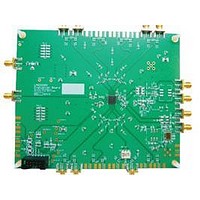
LMK03200EVAL
Description
BOARD EVALUATION LMK03200
Manufacturer
National Semiconductor
Specifications of LMK03200EVAL
Main Purpose
Timing, Clock Conditioner
Embedded
No
Utilized Ic / Part
LMK03200
Primary Attributes
3 LVDS & 5 LVPECL Outputs, Integrated PLL & VCO
Secondary Attributes
3.15 V ~ 3.45 V Supply
Silicon Manufacturer
National
Silicon Core Number
LMK03200
Kit Application Type
Clock & Timing
Application Sub Type
Precision Clock Conditioner
Kit Contents
Board, Cable
Lead Free Status / RoHS Status
Lead free / RoHS Compliant


Engaging 0-Delay Mode
To engage 0-Delay mode a two step programming sequence is followed as described in the datasheet.
Following this document’s “Read first, Basic Operation” section effectively completes step 1 with the
exception of setting 0-delay options in the Bits/Pins tab. When Ctrl-L is pressed all the registers listed
on the registers tab from R0 (INIT), R0 to R9, R11, R13 to R15 are programmed. Then step 2 is
performed and the outputs will be in 0-delay mode. The CodeLoader software simplifies step 2 by only
requiring the user to check the 0_DELAY_MODE checkbox on the Bits/Pins tab as the software
automatically reprograms PLL_N for the user. Clicking “Keyboard Controls”
same thing as pressing Ctrl-L.
The user must select a clock divide value which divides with no remainder into the PLL_N value of step
1 so that when 0_DELAY_MODE is enabled, the CLKout divider evenly divides into the PLL_N value.
If this is not done, CodeLoader will program the PLL VCO to the closest frequency which may cause
the device to loose lock. The two frequency loop equations which should result in the same VCO
frequency are shown below:
Step 1
To summarize step 1
Press Ctrl-L (same as “Keyboard Controls”
Step 2
Now that the part is operating on frequency, the second step enables the 0-delay mode.
When 0_DELAY_MODE is checked, the software will attempt to automatically re-program PLL_N with
the appropriate value so that lock is achieved given the selected CLKout divide. The software will also
attempt to warn the user of any errors. For example:
If 0_DELAY_MODE is enabled but the appropriate clock outputs are not enabled given FB_MUX
setting = CLKout5, the following warning will display:
OSCin Frequency / PLL_R * PLL_N = VCO Frequency
OSCin Frequency / PLL_R * PLL_N_New * CLKoutX_DIV = VCO Frequency
•
•
•
•
•
•
and
Load a default Mode
On the PLL tab setup OSCin frequency, PLL R, PLL N, VCO output frequency, etc. as desired.
On the Clock Outputs tab setup the clock outputs as desired.
On the Bits/Pins tab, set the 0-delay options as desired, this includes FB_MUX for selecting
feedback channel, PLL_MUX to set digital lock detect, and DLD_MODE2 set for alternate
digital lock detect mode.
OSCin_FREQ is set to the nearest MHz value of the OSCin frequency.
Note, register words (like R0, R1, R15, etc.) are loaded to the device when changes are made
to register bits (like PLL_N, CLKout3_EN, etc) assuming that the menu “Options” ->
“AutoReload with Changes,” is checked, which is its default setting. By pressing Ctrl-L
manually, this ensures all registers are loaded and in the proper order.
Check 0_DELAY_MODE on Bits/Pins tab
•
The lowest frequency must be feed back to PLL N, so CLKout5 or CLKout6 must be
programmed with the lowest frequency. If external feedback is used, the clock which
generates the signal for external feedback must be programmed with the lowest
frequency.
L M K 0 3 2 0 0
E V A L U A T I O N
Ensure that 0_DELAY_MODE is unchecked.
“Load Device”).
8
B O A R D
O P E R A T I N G
I N S T R U C T I O N S
“Load Device” is the
Ensure that
Related parts for LMK03200EVAL
Image
Part Number
Description
Manufacturer
Datasheet
Request
R

Part Number:
Description:
Precision 0-delay Clock Conditioner With Integrated Vco
Manufacturer:
National Semiconductor Corporation
Datasheet:

Part Number:
Description:
National Semiconductor [8-Bit D/A Converter]
Manufacturer:
National Semiconductor
Datasheet:
Part Number:
Description:
National Semiconductor [Media Coprocessor]
Manufacturer:
National Semiconductor
Datasheet:
Part Number:
Description:
Digitally Controlled Tone and Volume Circuit with Stereo Audio Power Amplifier, Microphone Preamp Stage and National 3D Sound
Manufacturer:
National Semiconductor
Datasheet:
Part Number:
Description:
Digitally Controlled Tone and Volume Circuit with Stereo Audio Power Amplifier, Microphone Preamp Stage and National 3D Sound
Manufacturer:
National Semiconductor
Datasheet:
Part Number:
Description:
AC97 Rev 2 Codec with Sample Rate Conversion and National 3D Sound
Manufacturer:
National Semiconductor
Part Number:
Description:
Manufacturer:
National Semiconductor
Datasheet:
Part Number:
Description:
Manufacturer:
National Semiconductor
Datasheet:
Part Number:
Description:
General Purpose, Low Voltage, Low Power, Rail-to-Rail Output Operational Amplifiers
Manufacturer:
National Semiconductor
Datasheet:
Part Number:
Description:
8-bit 20 MSPS flash A/D converter.
Manufacturer:
National Semiconductor
Datasheet:
Part Number:
Description:
Low Noise Quad Operational Amplifier
Manufacturer:
National Semiconductor
Datasheet:
Part Number:
Description:
Quad Differential Line Receivers
Manufacturer:
National Semiconductor
Datasheet:
Part Number:
Description:
Quad High Speed Trapezoidal? Bus Transceiver
Manufacturer:
National Semiconductor
Datasheet:
Part Number:
Description:
Dual Line Receiver
Manufacturer:
National Semiconductor
Datasheet: