LMK03200EVAL National Semiconductor, LMK03200EVAL Datasheet - Page 19
LMK03200EVAL
Manufacturer Part Number
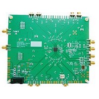
LMK03200EVAL
Description
BOARD EVALUATION LMK03200
Manufacturer
National Semiconductor
Specifications of LMK03200EVAL
Main Purpose
Timing, Clock Conditioner
Embedded
No
Utilized Ic / Part
LMK03200
Primary Attributes
3 LVDS & 5 LVPECL Outputs, Integrated PLL & VCO
Secondary Attributes
3.15 V ~ 3.45 V Supply
Silicon Manufacturer
National
Silicon Core Number
LMK03200
Kit Application Type
Clock & Timing
Application Sub Type
Precision Clock Conditioner
Kit Contents
Board, Cable
Lead Free Status / RoHS Status
Lead free / RoHS Compliant


L M K 0 3 2 0 0
E V A L U A T I O N
B O A R D
O P E R A T I N G
I N S T R U C T I O N S
The PLL tab shows a conventional PLL diagram along with the VCO Divider. It is important to
realize that the total effective N value is PLL N Counter * VCO Divider. This means that the
“channel spacing” is the Phase Detector Frequency * VCO Divider. Depending on the situation,
this may require the R Counter multiplied up by the value of the VCO Divider to achieve desired
VCO output frequencies. When 0-delay mode is active, the total effective N value is PLL N
Counter * Clock Output Divider * VCO Divider.
Figure 17 - PLL tab
Example: If the desired VCO output frequency was 1244.16 MHz, R would need to be increased
to 2 before 1253.88 MHz could be programmed because the VCO Divider of 2 would only allow
programming of 1244.16, 1263.6, 1283.04, etc. with a 9.72 MHz phase detector frequency. This
is because changing the N counter from 64 to 65 changes to total N by two, 128 to 130!
When in 0-Delay Mode, then selected channel divider is added to the divide on the feedback path
after VCO Divider. Refer to Figure 7 to see this illustrated.
19
Related parts for LMK03200EVAL
Image
Part Number
Description
Manufacturer
Datasheet
Request
R

Part Number:
Description:
Precision 0-delay Clock Conditioner With Integrated Vco
Manufacturer:
National Semiconductor Corporation
Datasheet:

Part Number:
Description:
National Semiconductor [8-Bit D/A Converter]
Manufacturer:
National Semiconductor
Datasheet:
Part Number:
Description:
National Semiconductor [Media Coprocessor]
Manufacturer:
National Semiconductor
Datasheet:
Part Number:
Description:
Digitally Controlled Tone and Volume Circuit with Stereo Audio Power Amplifier, Microphone Preamp Stage and National 3D Sound
Manufacturer:
National Semiconductor
Datasheet:
Part Number:
Description:
Digitally Controlled Tone and Volume Circuit with Stereo Audio Power Amplifier, Microphone Preamp Stage and National 3D Sound
Manufacturer:
National Semiconductor
Datasheet:
Part Number:
Description:
AC97 Rev 2 Codec with Sample Rate Conversion and National 3D Sound
Manufacturer:
National Semiconductor
Part Number:
Description:
Manufacturer:
National Semiconductor
Datasheet:
Part Number:
Description:
Manufacturer:
National Semiconductor
Datasheet:
Part Number:
Description:
General Purpose, Low Voltage, Low Power, Rail-to-Rail Output Operational Amplifiers
Manufacturer:
National Semiconductor
Datasheet:
Part Number:
Description:
8-bit 20 MSPS flash A/D converter.
Manufacturer:
National Semiconductor
Datasheet:
Part Number:
Description:
Low Noise Quad Operational Amplifier
Manufacturer:
National Semiconductor
Datasheet:
Part Number:
Description:
Quad Differential Line Receivers
Manufacturer:
National Semiconductor
Datasheet:
Part Number:
Description:
Quad High Speed Trapezoidal? Bus Transceiver
Manufacturer:
National Semiconductor
Datasheet:
Part Number:
Description:
Dual Line Receiver
Manufacturer:
National Semiconductor
Datasheet: