CDB5376 Cirrus Logic Inc, CDB5376 Datasheet - Page 35
CDB5376
Manufacturer Part Number
CDB5376
Description
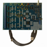
EVALUATION BOARD FOR CS5376
Manufacturer
Cirrus Logic Inc
Datasheets
1.CS5371A-ISZR.pdf
(32 pages)
2.CS4373A-ISZ.pdf
(34 pages)
3.CS5376A-IQZR.pdf
(106 pages)
4.CDB5378.pdf
(16 pages)
5.CDB5376.pdf
(80 pages)
6.CDB5376.pdf
(16 pages)
Specifications of CDB5376
Main Purpose
Seismic Evaluation System
Embedded
Yes, MCU, 8-Bit
Utilized Ic / Part
CS3301A, CS3302A, CS4373A, CS5372A, CS5376A
Primary Attributes
Quad Digital Filter
Secondary Attributes
Graphical User Interface, SPI™ & USB Interfaces
Processor To Be Evaluated
CS330x, CS4373A, CS537x
Interface Type
USB
Lead Free Status / RoHS Status
Contains lead / RoHS non-compliant
Lead Free Status / RoHS Status
Lead free / RoHS Compliant, Contains lead / RoHS non-compliant
Other names
598-1778


The VD and VCORE power supplies on CDB5376 include reverse-biased Schottkey diodes to ground to
protect against reverse voltages that could latch-up the CMOS components. Also included on VD and
VCORE are 100 uF bulk capacitors for bypassing and to help settle transients plus individual 0.1 uF by-
pass capacitors local to the digital power supply pins of each device.
2.5
2.5.1
CDB5376 layers 1 and 2 are dedicated as analog routing layers. All critical analog signal routes are on
these two layers. Some CPLD and microcontroller digital routes are also included on these layers away
from the analog signal routes.
CDB5376 layer 3 is dedicated for power supply routing. Each power supply net includes at least 100 µF
bulk capacitance as a charge well for settling transient current loads.
CDB5376 layer 4 is a solid ground plane without splits or routing. A soild ground plane provides the best
return path for bypassed noise to leave the system. No separate analog ground is required since analog
signals on CDB5376 are differentially routed.
CDB5376 layers 5 and 6 are dedicated as digital routing layers.
2.5.2
Analog signal routes on CDB5376 are differential with dedicated + and - traces. All source and return an-
alog signal currents are constrained to the differential pair route and do not return through the ground
plane. Differential traces are routed together with a minimal gap between them so that noise events affect
them equally and are rejected as common mode noise.
Analog signal connections into the CS3301A/02A amplifiers are 2-wire IN+ and IN- differential pairs, and
are routed as such. Analog signal connections out of the CS3301A/02A amplifiers and into the CS5372A
DS612DB3
PCB Layout
Layer Stack
Differential Pairs
Figure 4. Differential Pair Routing
IN+
IN-
CDB5376
35
Related parts for CDB5376
Image
Part Number
Description
Manufacturer
Datasheet
Request
R

Part Number:
Description:
Development Kit
Manufacturer:
Cirrus Logic Inc
Datasheet:
Part Number:
Description:
Development Kit
Manufacturer:
Cirrus Logic Inc
Datasheet:


Part Number:
Description:
High-efficiency PFC + Fluorescent Lamp Driver Reference Design
Manufacturer:
Cirrus Logic Inc
Datasheet:
Part Number:
Description:
Development Kit
Manufacturer:
Cirrus Logic Inc
Datasheet:
Part Number:
Description:
Development Kit
Manufacturer:
Cirrus Logic Inc
Datasheet:

Part Number:
Description:
Development Kit
Manufacturer:
Cirrus Logic Inc
Datasheet:
Part Number:
Description:
Development Kit
Manufacturer:
Cirrus Logic Inc
Datasheet:
Part Number:
Description:
Development Kit
Manufacturer:
Cirrus Logic Inc
Datasheet:
Part Number:
Description:
Development Kit
Manufacturer:
Cirrus Logic Inc
Datasheet:

Part Number:
Description:
EVALUATION BOARD FOR CS8427
Manufacturer:
Cirrus Logic Inc
Datasheet:

Part Number:
Description:
BOARD EVAL FOR CS8416 RCVR
Manufacturer:
Cirrus Logic Inc
Datasheet:

Part Number:
Description:
EVALUATION BOARD FOR CS8420
Manufacturer:
Cirrus Logic Inc
Datasheet:

Part Number:
Description:
KIT DEVELOPMENT EP9315 ARM9
Manufacturer:
Cirrus Logic Inc
Datasheet:

Part Number:
Description:
KIT DEVELOPMENT EP9302 ARM9
Manufacturer:
Cirrus Logic Inc
Datasheet: