CDB4270 Cirrus Logic Inc, CDB4270 Datasheet - Page 5
CDB4270
Manufacturer Part Number
CDB4270
Description
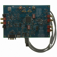
BOARD EVAL FOR CS4270 CODEC
Manufacturer
Cirrus Logic Inc
Datasheet
1.CDB4270.pdf
(50 pages)
Specifications of CDB4270
Main Purpose
Audio, CODEC
Embedded
Yes, FPGA / CPLD
Utilized Ic / Part
CS4270
Primary Attributes
Stereo, 24-Bit, 192 kHz Sample Rate
Secondary Attributes
I²S, S/PDIF Inputs and Outputs, Analog Inputs and Outputs, GUI
Description/function
Audio CODECs
Operating Supply Voltage
5 V
Product
Audio Modules
For Use With/related Products
CS4270
Lead Free Status / RoHS Status
Contains lead / RoHS non-compliant
Lead Free Status / RoHS Status
Lead free / RoHS Compliant, Contains lead / RoHS non-compliant
Other names
598-1002


DS686DB3
1. SYSTEM OVERVIEW
The CDB4270 evaluation board is an excellent tool for evaluating the CS4270 CODEC. The board features both
analog and digital audio interfaces along with an FPGA for data/clk routing and an on-board microprocessor for con-
figuration control. The board is easily configured in Software Mode using the supplied PC-to-DUT USB cable along
with the Windows-based GUI configuration software or in Hardware Mode using the on-board dip switches.
The CDB4270 schematic set has been partitioned into nine pages and is shown in
1.1
1.2
1.3
1.4
1.5
1.6
WARNING: Please refer to the CS4270 data sheet for allowable voltage levels.
Power
Power must be supplied to the evaluation board through the +5.0 V binding posts. The +5 V inputs must be
referenced to the single black binding post ground connector
Grounding and Power Supply Decoupling
To optimize performance, PC board designs for the CS4270 require careful attention to power supply,
grounding and signal routing arrangements.
connect for the CDB4270.
shows the top layout.
as close to the CS4270 as possible. Extensive use of ground plane fill in the evaluation board yields large
reductions in radiated noise.
FPGA
See
on the CDB4270.
CS4270 Audio CODEC
A complete description of the CS4270
The CS4270 codec performs stereo 24-bit A/D and D/A conversion at sample rates of up to 216 KHz. The
part accommodates I²S, Left-Justified and Right-Justified serial audio formats.
CS8406 Digital Audio Transmitter
A complete description of the CS8406 transmitter
dio interface are included in the CS8406 data sheet.
The CS8406 converts the PCM data from either the CS4270, the DSP Header, or the CS8416 to a standard
S/PDIF data stream. The CS8406 operates in either master or slave sub-clock mode and will accept either
a 128 Fs, 256 Fs, or 512 Fs master clock on the OMCK input pin. The device will operate in either the Left-
Justified or I²S interface data modes.
CS8416 Digital Audio Receiver
A complete description of the CS8416 receiver
interface are included in the CS8416 data sheet.
The CS8416 converts the input S/PDIF data stream into PCM data that can be used by the CS4270 and
CS8406. The device operates in either Master or Slave sub-clock modes and generates either a 128 Fs or
256 Fs master clock for output on the RMCK pin. Either Left-Justified or I²S interface output data formats
can be selected
“FPGA Overview” on page 9
Figure 77 on page 48
Figure 75 on page 46
for a complete description of the FPGA
(Figure 66 on page
shows the bottom layout. The decoupling capacitors are located
Figure 65 on page 36
(Figure 70 on page
shows the component placement.
(Figure 69 on page
37) is included in the CS4270 product data sheet.
(Figure 74 on page
shows the basic component/signal inter-
41) and a discussion of the digital audio
40) and a discussion of the digital au-
(Figure 72 on page
Figures 66
45).
Figure 76 on page 47
through 74.
43) that is used
CDB4270
5
Related parts for CDB4270
Image
Part Number
Description
Manufacturer
Datasheet
Request
R

Part Number:
Description:
Development Kit
Manufacturer:
Cirrus Logic Inc
Datasheet:
Part Number:
Description:
Development Kit
Manufacturer:
Cirrus Logic Inc
Datasheet:


Part Number:
Description:
High-efficiency PFC + Fluorescent Lamp Driver Reference Design
Manufacturer:
Cirrus Logic Inc
Datasheet:
Part Number:
Description:
Development Kit
Manufacturer:
Cirrus Logic Inc
Datasheet:
Part Number:
Description:
Development Kit
Manufacturer:
Cirrus Logic Inc
Datasheet:

Part Number:
Description:
Development Kit
Manufacturer:
Cirrus Logic Inc
Datasheet:
Part Number:
Description:
Development Kit
Manufacturer:
Cirrus Logic Inc
Datasheet:
Part Number:
Description:
Development Kit
Manufacturer:
Cirrus Logic Inc
Datasheet:
Part Number:
Description:
Development Kit
Manufacturer:
Cirrus Logic Inc
Datasheet:

Part Number:
Description:
EVALUATION BOARD FOR CS8427
Manufacturer:
Cirrus Logic Inc
Datasheet:

Part Number:
Description:
BOARD EVAL FOR CS8416 RCVR
Manufacturer:
Cirrus Logic Inc
Datasheet:

Part Number:
Description:
EVALUATION BOARD FOR CS8420
Manufacturer:
Cirrus Logic Inc
Datasheet:

Part Number:
Description:
KIT DEVELOPMENT EP9315 ARM9
Manufacturer:
Cirrus Logic Inc
Datasheet:

Part Number:
Description:
KIT DEVELOPMENT EP9302 ARM9
Manufacturer:
Cirrus Logic Inc
Datasheet: