CDB4270 Cirrus Logic Inc, CDB4270 Datasheet
CDB4270
Specifications of CDB4270


Related parts for CDB4270


CDB4270 Summary of contents
Page 1
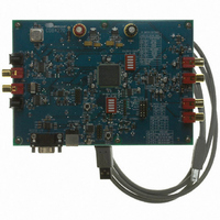
... Clocks /Data Osc. DSP HEADER http://www.cirrus.com Description Using the CDB4270 is an excellent way to evaluate the CS4270 CODEC. Other equipment required includes analog/digital audio sources/analyzer power sup- ply and a Windows-compatible PC for the GUI. System timing for the I²S, Left-Justified or Right-Justi- fied audio data formats can be provided by the CS4270, by the CS8416 device connected to the on- board DSP I/O header ...
Page 2
... CS8406 SDIN Source (Bits 1:0) ............................................................................................ 22 5.5.1 CS8416 RMCLK Divider Control (Bit 6) ................................................................................ 23 5.5.2 CS8416 Master/Slave Select (Bit 4) ...................................................................................... 23 5.5.3 CS8416 SDOUT Format Select (Bit 3) .................................................................................. 23 6. CDB4270 HARDWARE MODE SETTINGS ......................................................................................... 24 7. CDB CONNECTORS, SWITCHES, INDICATORS AND JUMPERS ................................................... 26 8. ADC PERFORMANCE PLOTS ............................................................................................................ 27 9. DAC PERFORMANCE PLOTS ............................................................................................................ 31 10 ...
Page 3
... Figure 2.ADC Dynamic Range .................................................................................................................... 7 Figure 3.Internal Sub-Clock Routing ........................................................................................................... 9 Figure 4.Internal Data Routing .................................................................................................................. 10 Figure 5.Internal Drivers ............................................................................................................................ 11 Figure 6.External MCLK Control ............................................................................................................... 12 Figure 7.CDB4270 Controls Tab ............................................................................................................... 14 Figure 8.Register Maps Tab - CS4270 ..................................................................................................... 15 Figure 9.Register Maps Tab - Board Configuration .................................................................................. 16 Figure 10.Register Maps Tab - GPIO ....................................................................................................... 17 Figure 11.FFT (- kHz) ................................................................................................................... 27 Figure 12 ...
Page 4
... Table 6. CS8406 OMCLK Frequency ....................................................................................................... 21 Table 7. CS8406 Master/Slave ................................................................................................................. 22 Table 8. CS8406 SDIN Format ................................................................................................................. 22 Table 9. CS8406 SDIN Source ................................................................................................................. 22 Table 10. CS8416 RMCLK Frequency ...................................................................................................... 23 Table 11. CS8416 Master/Slave ............................................................................................................... 23 Table 12. CS8416 SDOUT Format ........................................................................................................... 23 Table 13. CDB4270 Hardware Mode - Functional Description ................................................................. 24 Table 14. Connectors and Switches ......................................................................................................... 26 Table 15. Jumpers and Indicators ............................................................................................................. 26 4 CDB4270 DS686DB3 ...
Page 5
... SYSTEM OVERVIEW The CDB4270 evaluation board is an excellent tool for evaluating the CS4270 CODEC. The board features both analog and digital audio interfaces along with an FPGA for data/clk routing and an on-board microprocessor for con- figuration control. The board is easily configured in Software Mode using the supplied PC-to-DUT USB cable along with the Windows-based GUI configuration software or in Hardware Mode using the on-board dip switches ...
Page 6
... Vrms single-ended signal into the RCA connectors will drive the CS4270 inputs to full scale (1 Vrms). The input network on the CDB4270 was designed to demonstrate that the CS4270 will provide superior perfor- mance with up to 2.5 kΩ driving impedances (looking back from the CS4270 inputs) while allowing for 2 Vrms inputs ...
Page 7
... DS686DB3 Figure 1. ADC THD+N Figure 2. ADC Dynamic Range CDB4270 7 ...
Page 8
... The CS4270 analog outputs are AC-coupled and routed through a single-pole RC Low-Pass filter. 1.11 Control Port A graphical user interface is included with the CDB4270 to allow easy manipulation of the registers in the CS4270 (see the CS4270 data sheet for register descriptions and the page 18). The GUI will run on a standard Windows-based PC. Connecting a USB cable from J15 or an RS-232 cable to J16 and launching the Cirrus Logic FlexGUI software enables control and configura- tion of the board ...
Page 9
... FPGA-DUT-SCLK FPGA-DUT-LRCK HDR-SCLK HDR-LRCK FPGA-CS8406-LRCK FPGA-CS8406-SCLK CS8416-FPGA- LRCK CS8416-FPGA-SCLK SUB_CK[1:0] SUB_CK[1:0] CS8416-FPGA-SCLK CS8416-FPGA-LRCK FPGA-DUT-SCLK FPGA-DUT-LRCK FPGA-CS8406-SCLK FPGA-CS8406-LRCK HDR-LRCK HDR-SCLK Figure 3. Internal Sub-Clock Routing CDB4270 shows the MCLK routing to/from FPGA GUI section of this document for a CS4270 LRCK SCLK CS8406 LRCK SCLK 9 ...
Page 10
... Internal Data Routing Figure 4 shows the internal data routing topology between the CS4270, CS8416, CS8406 and the DSP Header. Refer to the FPGA GUI Register Description data routing register settings section of this document for a description of the audio Figure 4. Internal Data Routing CDB4270 6 DS686DB3 ...
Page 11
... MICRO-SDA/CCLK FPGA-SPI HDR-SDA/CDOUT MICRO-SCL/MISO HDR-SCL/CCLK FPGA-CS HDR-AD1/CDIN FPGA-AD0 FPGA-I2C HDR-AD2 FPGA-MOSI HDR-AD0/CS FPGA-AD1 FPGA-AD2 DS686DB3 FPGA FPGA-SPI FPGA-SPI FPGA-SPI FPGA-I2C FPGA-I2C FPGA-I2C Figure 5. Internal Drivers CDB4270 FPGA M1 M0 MDIV1 MDIV2 DIF FPGA-SW/HW I2C 11 ...
Page 12
... External MCLK Control Several sources for MCLK exist on the CDB4270. The crystal oscillator, Y1, will master the MCLK bus when no S/PDIF signal is input to the CS8416 (refer to the CS8416 data sheet for details on OMCK operation). When S/PDIF data is present at the CS8416 input, the CS8416 generates a master clock whenever its in- ternal PLL is locked to the incoming S/PDIF stream ...
Page 13
... CDB4270 and the host PC, run “FlexLoader.exe”. The software should automatically detect the board board selection dialog is displayed, select “CDB4270” from the list. Once loaded, all registers are set to their default state. Note: The board is automatically set to Software Control Mode once the serial or USB cable is installed and the GUI is up and running. The GUI’ ...
Page 14
... CDB4270 GUI Brief descriptions of the GUI tab views are provided below. The CDB4270 Controls tab provides high-level control of the CS4270, FPGA (Board Controls) and S/PDIF Tx and Rx devices. The “CS4270 Controls” group affects that device’s register settings. The “Board Con- trols” ...
Page 15
... For byte-wise modification, the desired hex value can be typed directly into the register address box in the register map. Refer to the CS4270 device data sheet register settings section and the FPGA reg- ister information in this document for register definitions. DS686DB3 Figure 8. Register Maps Tab - CS4270 CDB4270 15 ...
Page 16
... Figure 9. Register Maps Tab - Board Configuration 16 CDB4270 DS686DB3 ...
Page 17
... DS686DB3 Figure 10. Register Maps Tab - GPIO CDB4270 17 ...
Page 18
... HARDWARE MODE When the Flex GUI is not running when the USB or serial port cables are not connected to the CDB4270 from the PC, the board is automatically in Hardware Control Mode. When in this control mode, dip switches S1 and S2 control the board’s functionality. Note: Hardware Mode controls are a subset of Software Mode controls, and some FPGA or CS4270 register bits cannot be changed in Hardware Mode. See tings” ...
Page 19
... Table 1. Revision Number CDB4270 REV.2 REV.1 REV.0 Table 1. Revision Number Not Used Revision 1.1 Revision 1.2 Revision 1.3 Revision 1.4 Revision 1.5 Revision 1.6 Revision 1.7 ... Revision 1.15 ... Revision 15.9 Revision 15.10 Revision 15.11 Revision 15.12 Revision 15.13 Revision 15.14 Revision 15.15 ...
Page 20
... MCLK from Oscillator (through CS8416), MCLK to DSP Header Table 3. MCLK Source . SDIN/SDOUT Routing CS4270 SDOUT source to CS4270 SDIN CS8416 SDOUT source to CS4270 SDIN SDIN from DSP Header to CS4270 SDIN Connect GND to CS4270 SDIN Table 4. SDOUT Routing to DUT CDB4270 DUT_SDIO.0 SUB_CK.1 SUB_CK.0 shows the available settings. DS686DB3 ...
Page 21
... CS4270 and CS8416 are Slave to CS8406 - CS8406 is Master - DSP Header Sub-clocks are Outputs from CS8406 Table 5. Sub-Clock Routing TX_M/S TX_FMT Table 6 CS8406 OMCLK Frequency Table 6. CS8406 OMCLK Frequency CDB4270 2 1 Reserved TXSDIO.1 TXSDIO.0 shows the available settings. 256 x Fs 128 x Fs 512 x Fs 256 x Fs Table 5 ...
Page 22
... CS8406 Slave Mode CS8406 Master Mode Table 7. CS8406 Master/Slave Table 8. CS8406 SDIN Format 24-bit Left-Justified 24-bit I²S Table 8. CS8406 SDIN Format Table 9 shows the available settings. CS8406 SDIN Source CS4270 SDOUT CS8416 SDOUT SDIN from Header GND Table 9. CS8406 SDIN Source CDB4270 DS686DB3 ...
Page 23
... RX_M/S RX_FMT Table 10. CS8416 RMCLK Frequency 256 x Fs 128 x Fs Table 10. CS8416 RMCLK Frequency CS8416 Master/Slave CS8416 Slave Mode CS8416 Master Mode Table 11. CS8416 Master/Slave See.Table 12 CS8416 SDOUT Format 24-bit Left-Justified 24-bit I²S Table 12. CS8416 SDOUT Format CDB4270 Reserved Reserved Reserved 23 ...
Page 24
... When the Flex GUI is not used and there is no serial port communication to the board, all devices are in HW Mode. FPGA SW control is disabled in this condition, and DIP switches S1 and S2 on the CDB4270 set the FPGA Registers to control board functionality. Note that the CS8406 and CS8416 are reset when SW/HW from the microprocessor goes low (going from Mode) ...
Page 25
... Table 13. CDB4270 Hardware Mode - Functional Description 1. For other M1, M0, MDIV2, MDIV1 states, CS8406 OMCLK=256xFs and CS8416 RMCLK=256xFs. Note: Whenever changes are made to the S/PDIF Receiver (CS8416), the FPGA (for CS4270 Modes) generates a CS8416.RESET (CS8416 RESET) after the parameter is changed. Reg 03h (FPGA) shows the parameters that apply ...
Page 26
... J8, pins 2-3 *J3, pins 1-2 J3, pins 2-3 D3 present D1 present Table 15. Jumpers and Indicators CDB4270 SIGNAL PRESENT I²C Control Port signals I²C Control Port signals I²C Control Port signals FUNCTION SELECTED/INDICATION *Normal I²C/SPI Operation Connect to pins 2 (control) and 3 (gnd) for external control * MUTEA Enable ...
Page 27
... Figure 14. 48 kHz, THD+N vs. Input Freq + +35 +30 +25 +20 +15 + -10 -15 -20 -25 -30 -35 -40 -20 +0 -40 -140 Figure 16. 48 kHz, Fade-to-Noise Linearity CDB4270 50 100 200 500 Figure 12. FFT (-60 dB, 48 kHz) 100 200 500 -120 -100 -80 -60 -40 dBr 10k 20k 10k 20k - ...
Page 28
... B F -60 S -70 -80 -90 -100 -110 2k 5k 10k 20k 20 50 Figure 22. 96 kHz, THD+N vs. Input Freq CDB4270 100 200 500 Figure 18. 48 kHz, Crosstalk 50 100 200 500 Figure 20. FFT (-60 dB, 96 kHz) 100 200 500 DS686DB3 10k 20k ...
Page 29
... B F -80 S -90 -100 -110 -120 -130 -140 -150 10k 20k Figure 28. FFT (192 kHz, -60 dB) CDB4270 T -120 -100 -80 -60 -40 dBr 100 200 500 Figure 26. 96 kHz, Crosstalk 50 100 200 500 -20 +0 10k 20k 10k 20k ...
Page 30
... Figure 32. 192 kHz, Fade-to-Noise Linearity +0 -10 -20 -30 -40 -50 - -80 S -90 -100 -110 -120 -130 -140 -150 2k 5k 10k 20k 20 CDB4270 100 200 500 -120 -100 -80 -60 -40 dBr 50 100 200 500 Figure 34. 192 kHz, Crosstalk DS686DB3 10k 20k -20 +0 10k ...
Page 31
... Figure 38. FFT (48 kHz Out-of-Band, No Input) +0 -10 -20 -30 - -60 A -70 -80 -90 -100 -110 2k 5k 10k 20k -120 -100 Figure 40. 48 kHz, THD+N vs. Level CDB4270 100 200 500 10k Hz 40k 60k 80k 100k Hz -80 -60 -40 -20 dBFS 20k 120k +0 31 ...
Page 32
... Figure 44. 48 kHz, Impulse Response +0 -10 -20 -30 -40 -50 - -70 r -80 A -90 -100 -110 -120 -130 -140 -150 10k 20k Figure 46. FFT (96 kHz, -60 dB) CDB4270 100 200 500 10k Hz 1m 1.5m 2m 2.5m sec 100 200 500 10k Hz DS686DB3 20k 3m 20k ...
Page 33
... Figure 48. FFT (96 kHz Out-of-Band, No Input) +0 -10 -20 -30 - -60 A -70 -80 -90 -100 -110 2k 5k 10k 20k -120 -100 Figure 50. 96 kHz, THD+N vs. Level + -40 -20 +0 Figure 52. 96 kHz, Frequency Response CDB4270 40k 60k 80k 100k Hz -80 -60 -40 -20 dBFS 100 200 500 10k Hz 120k +0 20k 33 ...
Page 34
... Figure 56. FFT (192 kHz, -60 dB) +0 -10 -20 -30 -40 -50 - -70 r -80 A -90 -100 -110 -120 -130 -140 -150 2k 5k 10k 20k Figure 58. FFT (192 kHz Out-of-Band, No Input) CDB4270 500u 750u 1m 1.25m sec 100 200 500 20k 40k 60k 80k 100k Hz DS686DB3 1.5m 10k 20k 120k ...
Page 35
... Figure 60. 192 kHz, THD+N vs. Level + -40 - Figure 62. 192 kHz, Frequency Response 2 1.75 1.5 1.25 1 750m 500m 250m V 0 -250m -500m -750m -1 -1.25 -1.5 -1. 10k 20k Figure 64. 192 kHz, Impulse Response CDB4270 -80 -60 -40 -20 dBFS 100 200 500 10k Hz 200u 400u 600u sec +0 20k 35 ...
Page 36
BLOCK DIAGRAM Hardware Setup CS8406 S/PDIF Output Figure 19 MCLK BUS CS8416 S/PDIF Hardware Setup Input FPGA Clocks Figure 20 /Data Figure 22 Osc. Figure 21 DSP HEADER Figure 21 Figure 23 USB/Serial Control Port 2 I C/SPI Header ...
Page 37
SCHEMATICS Figure 66. CS4270 ...
Page 38
Figure 67. Analog Input ...
Page 39
Figure 68. Analog Output ...
Page 40
Figure 69. CS8406 S/PDIF Transmitter ...
Page 41
Figure 70. CS8416 S/PDIF Receiver ...
Page 42
Figure 71. Buffers - Clock/Data Routing ...
Page 43
Figure 72. FPGA ...
Page 44
Figure 73. USB/RS232 Microprocessor ...
Page 45
Figure 74. Power ...
Page 46
LAYOUT Figure 75. Silk Screen ...
Page 47
Figure 76. Top-Side Layer ...
Page 48
Figure 77. Bottom-Side Layer ...
Page 49
... There is no rework necessary when CS4270 C0 parts are installed on the Rev. B board. See CDB Data Sheet DS686DB2 when B0 parts are installed on the Rev. B board or DS686DB1 when A0 parts are installed on the Rev. A board. Also reference the Rev. A0, B0, and C0 chip Errata at http://www.cirrus.com/en/support. Select Errata from the product information categories shown. DS686DB3 CDB4270 49 ...
Page 50
... Cirrus Logic, Cirrus, and the Cirrus Logic logo designs, and Popguard are trademarks of Cirrus Logic, Inc. All other brand and product names in this document may be trademarks or service marks of their respective owners. I² registered trademark of Philips Semiconductor. SPI is a trademark of Motorola, Inc. Windows is a registered trademark of Microsoft Corporation. 50 Changes www.cirrus.com. CDB4270 DS686DB3 ...