CDB4270 Cirrus Logic Inc, CDB4270 Datasheet - Page 13
CDB4270
Manufacturer Part Number
CDB4270
Description
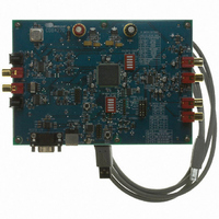
BOARD EVAL FOR CS4270 CODEC
Manufacturer
Cirrus Logic Inc
Datasheet
1.CDB4270.pdf
(50 pages)
Specifications of CDB4270
Main Purpose
Audio, CODEC
Embedded
Yes, FPGA / CPLD
Utilized Ic / Part
CS4270
Primary Attributes
Stereo, 24-Bit, 192 kHz Sample Rate
Secondary Attributes
I²S, S/PDIF Inputs and Outputs, Analog Inputs and Outputs, GUI
Description/function
Audio CODECs
Operating Supply Voltage
5 V
Product
Audio Modules
For Use With/related Products
CS4270
Lead Free Status / RoHS Status
Contains lead / RoHS non-compliant
Lead Free Status / RoHS Status
Lead free / RoHS Compliant, Contains lead / RoHS non-compliant
Other names
598-1002


DS686DB3
3. SOFTWARE MODE
The CDB4270 uses a Microsoft Windows-based GUI (download from Cirrus web site), which allows control of the
CS4270 and FPGA registers. Interface to the GUI is provided via USB or RS-232 serial connection. Once the ap-
propriate cable is connected between the CDB4270 and the host PC, run “FlexLoader.exe”. The software should
automatically detect the board. If a board selection dialog is displayed, select “CDB4270” from the list. Once loaded,
all registers are set to their default state. Note: The board is automatically set to Software Control Mode once the
serial or USB cable is installed and the GUI is up and running. The GUI’s “File” menu provides the ability to save
and load script files containing all of the register settings. Sample script files for basic mode operation can be down-
loaded from the archive at www.cirrus.com.
3.1
3.1.1
3.1.2
3.1.3
3.1.4
CDB4270 Control Scripts
Brief descriptions of the supplied scripts are given below.
S/PDIF In, Analog Out
When the SPDIF_IN_AOUT.FGS script is run, the CS8416 is the sub-clock (SCLK and LRCK) master and
all other devices including the DSP Header are slaves. The CS8416 provides MCLK recovered from the
S/PDIF data and SDOUT to the CS4270 DAC, DSP Header and CS8406.
Analog In, S/PDIF Out
When the AIN_SPDIF_OUT.FGS script is run, the crystal oscillator is the MCLK master. The CS8416
passes the clock from the crystal oscillator, Y1, through to the RMCK output (Note: the S/PDIF input must
be disconnected) to the CS4270, the CS8406 and the DSP Header. The CS4270 provides SDOUT to the
CS8406 and the DSP Header. The CS8406 generates sub-clocks derived from the CS4270 data and is
the sub-clock master. All other devices including the DSP Header are sub-clock slave devices.
Analog In, Analog Out (Digital Loop-Back)
When the AIN_AOUT.FGS script is run, the crystal oscillator is the MCLK master. The CS8416 passes
the clock from the crystal oscillator, Y1, through to the RMCK output (Note: the S/PDIF input must be dis-
connected) to the CS4270, the CS8406 and the DSP Header. The CS8416 generates sub-clocks derived
from the crystal oscillator and is the sub-clock master. All other devices and the DSP Header are sub-
clock slave devices. SDOUT from the CS4270 ADC is routed through the FPGA to the CS4270 DAC, to
the DSP Header and to the CS8406.
DSP In, Analog Out
When the DSP_IN_AOUT.FGS script is run, the DSP Header is the MCLK, sub-clock and data master
and all other devices are slaves. SDOUT at the header is the CS4270 SDOUT.
CDB4270
13
Related parts for CDB4270
Image
Part Number
Description
Manufacturer
Datasheet
Request
R

Part Number:
Description:
Development Kit
Manufacturer:
Cirrus Logic Inc
Datasheet:
Part Number:
Description:
Development Kit
Manufacturer:
Cirrus Logic Inc
Datasheet:


Part Number:
Description:
High-efficiency PFC + Fluorescent Lamp Driver Reference Design
Manufacturer:
Cirrus Logic Inc
Datasheet:
Part Number:
Description:
Development Kit
Manufacturer:
Cirrus Logic Inc
Datasheet:
Part Number:
Description:
Development Kit
Manufacturer:
Cirrus Logic Inc
Datasheet:

Part Number:
Description:
Development Kit
Manufacturer:
Cirrus Logic Inc
Datasheet:
Part Number:
Description:
Development Kit
Manufacturer:
Cirrus Logic Inc
Datasheet:
Part Number:
Description:
Development Kit
Manufacturer:
Cirrus Logic Inc
Datasheet:
Part Number:
Description:
Development Kit
Manufacturer:
Cirrus Logic Inc
Datasheet:

Part Number:
Description:
EVALUATION BOARD FOR CS8427
Manufacturer:
Cirrus Logic Inc
Datasheet:

Part Number:
Description:
BOARD EVAL FOR CS8416 RCVR
Manufacturer:
Cirrus Logic Inc
Datasheet:

Part Number:
Description:
EVALUATION BOARD FOR CS8420
Manufacturer:
Cirrus Logic Inc
Datasheet:

Part Number:
Description:
KIT DEVELOPMENT EP9315 ARM9
Manufacturer:
Cirrus Logic Inc
Datasheet:

Part Number:
Description:
KIT DEVELOPMENT EP9302 ARM9
Manufacturer:
Cirrus Logic Inc
Datasheet: