AD9520-4/PCBZ Analog Devices Inc, AD9520-4/PCBZ Datasheet - Page 4
AD9520-4/PCBZ
Manufacturer Part Number
AD9520-4/PCBZ
Description
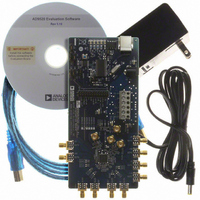
BOARD EVAL FOR AD9520-4
Manufacturer
Analog Devices Inc
Specifications of AD9520-4/PCBZ
Design Resources
Synchronizing Multiple AD9910 1 GSPS Direct Digital Synthesizers (CN0121) Phase Coherent FSK Modulator (CN0186)
Main Purpose
Timing, Clock Generator
Embedded
No
Utilized Ic / Part
AD9520-4
Primary Attributes
1.4 ~ 1.8 GHz Output Frequency
Secondary Attributes
Accepts CMOS, LVDS, or LVPECL References Up to 250 MHz
Silicon Manufacturer
Analog Devices
Application Sub Type
PLL Clock Synthesizer
Kit Application Type
Clock & Timing
Silicon Core Number
AD9520-0, AD9520-2, AD9520-2
Silicon Family Name
AD9520-X
Rohs Compliant
Yes
Lead Free Status / RoHS Status
Lead free / RoHS Compliant


AD9520-4
SPECIFICATIONS
Typical (typ) is given for VS = VS_DRV = 3.3 V ± 5%; VS ≤ VCP ≤ 5.25 V; T
noted. Minimum (min) and maximum (max) values are given over full VS and T
POWER SUPPLY REQUIREMENTS
Table 1.
Parameter
VS
VS_DRV
VCP
RSET Pin Resistor
CPRSET Pin Resistor
BYPASS Pin Capacitor
PLL CHARACTERISTICS
Table 2.
Parameter
VCO (ON-CHIP)
REFERENCE INPUTS
Frequency Range
VCO Gain (K
Tuning Voltage (V
Frequency Pushing (Open-Loop)
Phase Noise @ 1 kHz Offset
Phase Noise @ 100 kHz Offset
Phase Noise @ 1 MHz Offset
Differential Mode (REFIN, REFIN)
Dual Single-Ended Mode (REF1, REF2)
Input Frequency
Input Sensitivity
Self-Bias Voltage, REFIN
Self-Bias Voltage, REFIN
Input Resistance, REFIN
Input Resistance, REFIN
Input Frequency (AC-Coupled)
Input Frequency (AC-Coupled)
Input Frequency (DC-Coupled)
Input Sensitivity (AC-Coupled
Input Sensitivity (AC-Coupled
Input Logic High, DC Offset Off
Input Logic Low, DC Offset Off
Input Current
Input Capacitance
with DC Offset Off
with DC Offset On
with DC Offset Off )
with DC Offset On)
VCO
)
T
)
Min
3.135
2.375
VS
Typ
3.3
4.12
5.1
220
Max
3.465
VS
5.25
1.30
4.4
10
0.55
1.5
Min
1400
0.5
0
1.34
4.0
0
2.0
−100
Unit
V
V
V
kΩ
kΩ
nF
Typ
35
1
−58
−111
−130
280
1.60
1.50
4.8
5.3
2
This is nominally 2.5 V to 3.3 V ± 5%
This is nominally 3.3 V to 5.0 V ± 5%
Test Conditions/Comments
3.3 V ± 5%
Sets internal biasing currents; connect to ground
Sets internal CP current range, nominally 4.8 mA (CP_lsb = 600 μA); actual
current can be calculated by: CP_lsb = 3.06/CPRSET; connect to ground
Bypass for internal LDO regulator; necessary for LDO stability; connect to ground
Rev. 0 | Page 4 of 84
Max
1800
VCP −
0.5
250
1.75
1.60
5.9
6.4
250
250
250
3.28
2.78
0.8
+100
Unit
MHz
MHz/V
V
MHz/V
dBc/Hz
dBc/Hz
dBc/Hz
MHz
mV p-p
V
V
kΩ
kΩ
MHz
MHz
MHz
V p-p
V p-p
V
V
μA
pF
A
= 25°C; RSET = 4.12 kΩ; CPRSET = 5.1 kΩ, unless otherwise
A
(−40°C to +85°C) variation.
Test Conditions/Comments
See Figure 13
VCP ≤ VS when using internal VCO
f = 1625 MHz
f = 1625 MHz
f = 1625 MHz
Differential mode (can accommodate single-ended
input by ac grounding undriven input)
Frequencies below about 1 MHz should be dc-coupled;
be careful to match V
Self-bias voltage of REFIN
Self-bias voltage of REFIN
Self-biased
Self-biased
Two single-ended CMOS-compatible inputs
Slew rate must be > 50 V/μs
Slew rate must be > 50 V/μs, and input amplitude
sensitivity specification must be met; see input sensitivity
VIH should not exceed VS
VIH should not exceed VS
Each pin, REFIN (REF1)/REFIN (REF2)
See Figure 8
Slew rate > 50 V/μs; CMOS levels
1
1
CM
(self-bias voltage)
1
1
Related parts for AD9520-4/PCBZ
Image
Part Number
Description
Manufacturer
Datasheet
Request
R

Part Number:
Description:
12/24 Channel Clock Gen 2,0GH
Manufacturer:
Analog Devices Inc
Datasheet:

Part Number:
Description:
12/24 Channel Clock Gen 2,0GH
Manufacturer:
Analog Devices Inc
Datasheet:
Part Number:
Description:
12/24 Channel Clock Gen 2,0GH
Manufacturer:
Analog Devices Inc
Datasheet:
Part Number:
Description:
12/24 Channel Clock Gen 2,0GH
Manufacturer:
Analog Devices Inc
Datasheet:
Part Number:
Description:
12/24 Channel Clock Gen 2,0GH
Manufacturer:
Analog Devices Inc
Datasheet:
Part Number:
Description:
Clock IC With 2.8GHz On-chip VCO
Manufacturer:
Analog Devices Inc
Datasheet:
Part Number:
Description:
Lock IC With 2.8GHz On-chip VCO
Manufacturer:
Analog Devices Inc
Datasheet:
Part Number:
Description:
12/24 Channel Clock Gen 2,5 GHz VCO
Manufacturer:
Analog Devices Inc
Datasheet:
Part Number:
Description:
12/24 Channel Clock Distribution W/ On-C
Manufacturer:
Analog Devices Inc
Datasheet:
Part Number:
Description:
12/24 Channel Clock Gen 2,25GH
Manufacturer:
Analog Devices Inc
Datasheet:
Part Number:
Description:
12/24 Channel Clock Distribution W/ On-C
Manufacturer:
Analog Devices Inc
Datasheet:
Part Number:
Description:
12/24 Channel Clock Distribution W/ On-C
Manufacturer:
Analog Devices Inc
Datasheet:
Part Number:
Description:
Clock IC With 1.6GHz On-chip VCO
Manufacturer:
Analog Devices Inc
Datasheet:
Part Number:
Description:
Clock IC With 1.6GHz On-chip VCO
Manufacturer:
Analog Devices Inc
Datasheet:
Part Number:
Description:
12/24-Output Clock Generator
Manufacturer:
Analog Devices Inc
Datasheet: