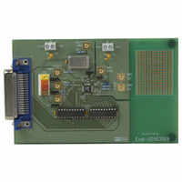
EVAL-AD9830EBZ Analog Devices Inc, EVAL-AD9830EBZ Datasheet - Page 11
EVAL-AD9830EBZ
Manufacturer Part Number
EVAL-AD9830EBZ
Description
BOARD EVALUATION AD9830
Manufacturer
Analog Devices Inc
Specifications of EVAL-AD9830EBZ
Main Purpose
Timing, Direct Digital Synthesis (DDS)
Utilized Ic / Part
AD9830
Lead Free Status / RoHS Status
Lead free / RoHS Compliant
Secondary Attributes
-
Embedded
-
Primary Attributes
-
Lead Free Status / Rohs Status
Supplier Unconfirmed


REV. A
full-scale voltage developed across it does not exceed the voltage
compliance range. Since full-scale current is controlled by R
adjustments to R
However, if the DAC full-scale output current is significantly less
than 20 mA, the linearity of the DAC may degrade.
DSP and MPU Interfacing
The AD9830 has a parallel interface, with 16 bits of data being
loaded during each write cycle.
The frequency or phase registers are loaded by asserting the WR
signal. The destination register for the 16-bit data is selected
using the address inputs A0, A1 and A2. The phase registers
are 12 bits wide so, only the 12 LSBs need to be valid—the
4 MSBs of the 16 bit word do not have to contain valid data.
Data is loaded into the AD9830 by pulsing WR low, the data
being latched into the AD9830 on the rising edge of WR. The
values of inputs A0, A1 and A2 are also latched into the
AD9830 on the WR rising edge. The appropriate register is up-
dated on the next MCLK rising edge. To ensure that the
AD9830 contains valid data at the rising edge of MCLK, the
rising edge of the WR pulse should not coincide with the rising
MCLK edge. The WR pulse must occur several nanoseconds
before the MCLK rising edge. If the WR rising edge occurs at
the MCLK rising edge, there is an uncertainty of one MCLK
cycle regarding the loading of the destination register—the desti-
nation register may be loaded with the new data immediately or
the destination register may be updated on the next MCLK ris-
ing edge. To avoid any uncertainty, the times listed in the speci-
fications should be complied with.
SET
can balance changes made to the load resistor.
V
OUT
CHANGE FSELECT
= V
Figure 23. Flow Chart for AD9830 Initialization and Operation
REFIN
*8*R
PHASEREG<3:0> = DELTA PHASE<0, 1, 2, 3>
OUT
/R
SET*
NO
NO
FREG<0> = f
FREG<1> = f
PHASEREG<0, 1, 2, 3> = 0
SELECT DATA SOURCES
WAIT 6 MCLK CYCLES
(1 + SIN(2 (FREG*f
SET PSEL0, PSEL1
CHANGE PHASE?
CHANGE FOUT?
CHANGE FREG?
FREG<0, 1> = 0
SET FSELECT
DAC OUTPUT
DATA WRITE
DATA WRITE
RESET
OUT
OUT
YES
YES
NO
0/f
1/f
MCLK
MCLK
SET
MCLK
*2
*2
,
YES
32
32
–11–
CHANGE PHASEREG?
*t/2
32
FSELECT, PSEL0 and PSEL1 are sampled on the MCLK
rising edge. Again, these inputs should be valid when an
MCLK rising edge occurs as there will be an uncertainty of one
MCLK cycle introduced otherwise. When these inputs change
value, there will be a pipeline delay before control is transferred
to the selected register—there will be a pipeline delay before the
analog output is controlled by the selected register. Similarly,
there is a delay when a new word is written to a register. PSEL0,
PSEL1, FSELECT and WR have latencies of six MCLK cycles.
The flow chart in Figure 23 shows the operating routine for the
AD9830. When the AD9830 is powered up, the part should be
reset using RESET. This will reset the phase accumulator to
zero so that the analog output is at midscale. RESET does not
reset the phase and frequency registers. These registers will con-
tain invalid data and, therefore, should be set to zero by the user.
The registers to be used should be loaded, the analog output be-
ing f
the selected frequency register. This signal will be phase shifted
by an amount 2 /4096 PHASEREG where PHASEREG is the
value contained in the selected phase register. When FSELECT,
PSEL0 and PSEL1 are programmed, there will be a pipeline de-
lay of approximately 6 MCLK cycles before the analog output
reacts to the change on these inputs.
+ PHASEREG/2
MCLK
YES
/2
32
12
)))
NO
FREG where FREG is the value contained in
CHANGE PSEL0, PSEL1
AD9830
Related parts for EVAL-AD9830EBZ
Image
Part Number
Description
Manufacturer
Datasheet
Request
R


Part Number:
Description:
BOARD EVAL FOR SI270X-A
Manufacturer:
Silicon Laboratories Inc
Datasheet:

Part Number:
Description:
BUCK CONV REF DESIGN KIT IP1201
Manufacturer:
International Rectifier
Datasheet:
Part Number:
Description:
BOARD DEMO SYNC DUAL BUCK CNVTER
Manufacturer:
International Rectifier
Datasheet:
Part Number:
Description:
BOARD DEMO SYNC BUCK CONVETER
Manufacturer:
International Rectifier
Datasheet:

Part Number:
Description:
EVALBOARD/EB Omnidirectional microphone - Analog
Manufacturer:
Analog Devices
Datasheet:
Part Number:
Description:
EVALBOARD/EB Omnidirectional microphone - Analog
Manufacturer:
Analog Devices
Datasheet:


Part Number:
Description:
BOARD EVAL LED DRIVER LT3756
Manufacturer:
Linear Technology
Datasheet:

Part Number:
Description:
BOARD EVAL FOR AD7741/7742
Manufacturer:
Analog Devices Inc
Datasheet:

Part Number:
Description:
±1.7g Dual-Axis IMEMS Accelerometer Evaluation Board
Manufacturer:
Analog Devices Inc
Datasheet:

Part Number:
Description:
IC MULTIPLIER ANALOG 8-SOIC T/R
Manufacturer:
Analog Devices Inc
Datasheet:

Part Number:
Description:
IC ANALOG MULTIPLIER 8-DIP
Manufacturer:
Analog Devices Inc
Datasheet:
Part Number:
Description:
IC ANALOG MULTIPLIER 8-SOIC
Manufacturer:
Analog Devices Inc
Datasheet:
Part Number:
Description:
IC ANALOG MULTIPLIER 8-DIP
Manufacturer:
Analog Devices Inc
Datasheet: